Chinese semiconductor thread II

tokenanalyst

Lieutenant General
Registered Member

Lehman Optoelectronics launches its third-generation home giant screen product, ushering in the era of widespread adoption of Micro LED home giant screens.​


Lehman Optoelectronics unveiled its third-generation Micro LED home giant screens at a launch event in Shenzhen, marking the official beginning of widespread adoption of ultra-large home displays. The company introduced two flagship models: the LV135 Max (135-inch, 4K) and LV163 Max (163-inch, 4K), priced at ¥199,999 and ¥239,999 respectively dramatically undercutting the previous industry barrier of over ¥500,000 for similar screens.

Available for pre-order via JD.com and Tmall, with shipments starting late March, these screens leverage pixel-level self-illumination, modular splicing, and low power consumption to deliver IMAX-like quality in the living room embodying Lehman’s vision: “The screen is the wall, the view is the world.”

Driven by national ultra-high-definition (4K/8K) content policies and consumer demand, Micro LED’s superior contrast, color accuracy, and durability make it the ideal technology for giant home displays. The products enable immersive “virtual reality” experiences allowing users to feel seasons change or explore global landscapes without leaving home.

Industry experts hail this as a pivotal moment transitioning Micro LED from commercial to consumer markets, unlocking a trillion-yuan blue ocean for China’s LED industry. With the Chinese home display market still dominated by 65–85-inch TVs, the 135-inch+ segment is poised for explosive growth over the next 3–5 years.

Lehman’s breakthroughs in cost reduction, supply chain integration, and scenario innovation have shattered previous adoption barriers — cost, product feasibility, content availability, and public awareness positioning the company as a leader in reshaping home lifestyles and accelerating dual upgrades across the display industry chain.

1769087397778.png

Please, Log in or Register to view URLs content!
 

tokenanalyst

Lieutenant General
Registered Member

Mingjia Semiconductor completes financing of over 100 million yuan to accelerate the mass production of 6-inch gallium oxide substrates.​


Beijing Mingjia Semiconductor Co., Ltd. successfully closed its A++ equity financing round, raising 110 million yuan (~$15.2 million USD), bringing its total funding to nearly 400 million yuan across five rounds. Led by investors including Pengcheng Venture Capital, Chengdu Science & Tech VC, Tianying Capital, Guoyu Fund, and Hongtai Fund, the company was valued at 910 million yuan post-money.

The funds will accelerate the mass production of 6-inch gallium oxide (Ga₂O₃) substrates a critical breakthrough enabling large-scale wafer fabrication for ultra-wide bandgap (UWB) semiconductors. Mingjia plans to expand its pilot lines with 20 new equipment units, boosting GaO substrate capacity to 30,000 wafers annually, while also developing 2–4 inch lines and scaling indium phosphide (InP) polycrystalline production.
1769088167740.png

This milestone marks Mingjia’s transition from R&D to industrialization, with signing ceremonies attended by Shunyi District officials and over 20 partners including investors, banks, and supply chain collaborators solidifying its ecosystem.​

Please, Log in or Register to view URLs content!
 

tokenanalyst

Lieutenant General
Registered Member
Shanghai Institute of Optics and Fine Mechanics has made progress in the field of adaptive interferometry detection of freeform surface optical elements.

Recently, the research team led by Professor Liu Shijie of the Optical Detection and Characterization Center of the High Power Laser Components Technology and Engineering Department of the Shanghai Institute of Optics and Fine Mechanics, Chinese Academy of Sciences, has made new progress in adaptive interferometry detection of optical components with large deviations from freeform surfaces. The relevant results were published in Optics Express under the title " Interferogram-free adaptive wavefront interferometry: fourier spot analysis enhancing adaptive compensation performance" .

To address the problem that traditional adaptive wavefront interferometry ( AWI ) heavily relies on interference fringe reconstruction and identification, making it ineffective in detecting large-area deviations from optical elements, this study proposes an interference-free adaptive wavefront interferometry ( IF-AWI ) based on Fourier spot ( FS ) analysis . This method completely eliminates the dependence on interference fringes, phase shift, and phase unwrapping during adaptive compensation. It guides the optimization direction by analyzing the Fourier spot intensity distribution, thus achieving stable and efficient wavefront compensation and measurement even when interference fringes cannot be formed or are severely missing.

To further improve optimization efficiency and convergence performance, the research team introduced a Runge–Kutta -based intelligent optimization algorithm, which achieves a good balance between global search capability and local convergence speed. This method can successfully compensate for freeform wavefronts with peak-to-valley values exceeding 100λ and root mean square values exceeding 20λ within about 60 iterations.

This achievement breaks through the fundamental limitation of traditional adaptive interferometry on the quality of interference fringes, significantly expands the measurable dynamic range of freeform surfaces, provides a brand-new technical path for the inspection of freeform surfaces in polishing, and has important application value for the manufacturing and inspection of high-end optical components.

Please, Log in or Register to view URLs content!
 

tokenanalyst

Lieutenant General
Registered Member

GigaDevice Announces New Generation GD32H7 Series MCUs​


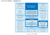
GigaDevice has launched its new GD32H7 series of ultra-high-performance microcontrollers, built on the Arm® Cortex®-M7 core and clocked at up to 750MHz. The series comprises two distinct families: the GD32H789/779 for general-purpose high-performance applications and the GD32H78E/77E, which integrate EtherCAT® slave controllers for real-time industrial automation. These MCUs are engineered to deliver exceptional computational power with a unique 640KB Tightly Coupled Memory (TCM) that operates at CPU speed, enabling zero-wait instruction and data access a critical advantage for time-sensitive tasks and complex algorithm execution.
1769088925928.png
The GD32H7 series offers industry-leading memory configurations, including up to 2MB of Execution Flash, 8MB of Storage Flash, and 1.2MB of SRAM, making it ideal for applications requiring large code bases and high-speed data buffering. Its architecture ensures seamless continuity in performance, allowing sustained computational output without bottlenecks. Coupled with optimized power efficiency, the series sets a new standard for balancing raw processing capability with low dynamic power consumption essential for both high-end industrial systems and energy-conscious portable devices.

To support advanced system expansion, the GD32H7 MCUs feature dual OSPI interfaces capable of 200MHz operation with Double Data Rate (DTR) mode, enabling direct, high-speed connectivity to external memory types such as PSRAM, HyperRAM, NAND, and NOR Flash. This flexibility, combined with integrated real-time communication capabilities, makes the GD32H7 series a compelling foundation for next-generation applications in servo control, digital power supplies, smart home systems, and fire protection empowering developers to build faster, smarter, and more responsive intelligent equipment.

Please, Log in or Register to view URLs content!


tokenanalyst

Lieutenant General
Registered Member

With an investment exceeding 300 million yuan, Jingce Semiconductor, a leading domestic metrology equipment company has commenced construction on its Shanghai base.​


According to reports, on the morning of January 16, the R&D headquarters and equipment manufacturing base project of Shanghai Jingce Semiconductor Technology Co., Ltd. officially broke ground. This marks a new stage of development for this leading company in the field of semiconductor testing equipment, which is deeply rooted in Qingpu District under the precise service and support of the Shixi Software and Information Park. It also adds new momentum to the construction of the Yangtze River Delta innovation hub.

Located in the Shixi Software and Information Park in Qingpu District, the project covers an area of 26.8 acres and represents a total investment of over 300 million yuan. Upon completion, it will become a comprehensive base integrating R&D, production, and experimentation, further strengthening the park's core hub role in the integrated circuit industry chain. The project took only 10 days from land acquisition to obtaining a construction permit, demonstrating the "Qingpu speed" and precise service.

Shanghai Jingce Semiconductor Technology Co., Ltd. is a holding subsidiary of Wuhan Jingce Electronics Group Co., Ltd. Established in July 2018, the company focuses on semiconductor front-end process measurement technology and has mastered key core technologies such as spectral scattering measurement, optical interferometry, and electron beam/ion beam imaging. Its products cover film thickness measurement, optical critical dimension (OCD) measurement, electron beam defect detection and other equipment, which are widely used in advanced storage, HBM (high bandwidth memory) and other fields.

As a leading enterprise in China's semiconductor metrology field, the company has secured orders exceeding 400 million yuan in recent years. Its products have been delivered in batches to numerous well-known domestic semiconductor companies, and its technological capabilities and product stability have been highly recognized by customers. The company plans to invest approximately 350 million yuan in a second-phase laboratory expansion project, adding cleanrooms, office and laboratory areas, and other facilities to further enhance its R&D and production capabilities and alleviate the resource constraints of its existing production lines. Haijing Measurement Semiconductor Technology Co., Ltd. is a leading enterprise in China's semiconductor metrology field, and through technological innovation and capacity expansion, it is gradually enhancing its competitiveness in the global market.

Please, Log in or Register to view URLs content!
 
Last edited:
Top