Chinese semiconductor thread II

tokenanalyst

Lieutenant General
Registered Member

Shangyang Software, in collaboration with Xinshun Microelectronics, has completed a comprehensive system upgrade, creating the "most powerful brain" for automotive-grade wafer manufacturing.​


Shangyang Software and Jiangsu Xinshun Microelectronics announced the successful completion of a major manufacturing system upgrade described as creating the “most powerful brain” for automotive-grade semiconductor wafers.

Building on over 20 years of collaboration, Shangyang Software delivered a comprehensive overhaul of Xinshun Micro’s Manufacturing Execution System (MES) and pioneered the deployment of an advanced Equipment Execution System (EES), forming an integrated CIM (Computer-Integrated Manufacturing) solution tailored for high-reliability automotive production.​
  • Equipment Automation Platform (EAP): Enabled end-to-end digital control of wafer equipment from real-time monitoring and predictive anomaly alerts to closed-loop process parameter adjustment eliminating manual inspections and reducing human error.​
  • 100% Automotive-Grade Compliance: Fully integrated all automotive production equipment to ensure end-to-end traceability, capturing every process parameter and equipment log from raw material to finished wafer meeting the stringent stability and consistency demands of automotive semiconductors.​
  • Performance Gains:
    • Increase product yield and qualification rates​
    • Reduced scrap and rework rates​
    • Decreased production cycle times​
    • Increase overall Factory Effectiveness (OFE) and equipment utilization​
The upgrade transforms Xinshun Micro’s manufacturing into a data-driven, transparent, and standardized operation — shifting from reactive to predictive and precise control.

Shangyang Software emphasized its “technology adapted to needs” philosophy, aligning every system enhancement with Xinshun Micro’s operational realities and strategic goals. This project underscores a broader mission: empowering Chinese semiconductor firms to lead in high-end markets like automotive and industrial-grade chips.

Looking ahead, Shangyang Software will continue advancing CIM solutions to help domestic manufacturers strengthen global competitiveness and elevate “Made in China” in the critical semiconductor supply chain.

iangsu Xinshun Microelectronics Co., Ltd. specializes in the research, development, production, sales, and service of semiconductor chips. Currently, it operates one 5-inch and one 6-inch chip production line, providing customers with over 2,000 different specifications and models across six major series. Its products are widely used in energy conversion, green lighting, rail transportation, smart grids, smart homes, computer equipment, mobile devices, communications, and home appliances, covering numerous fields within the electronics and information industry.​

Please, Log in or Register to view URLs content!
 

tokenanalyst

Lieutenant General
Registered Member

Shangyang Software officially launched the CIM system for Visionox Technology's 12-inch silicon-based OLED fully automated production line.


Recently, Shangyang Software officially launched the CIM (Computer Integrated Manufacturing) software system for Visionox's 12-inch silicon-based OLED fully automated production line. This project launch marks another breakthrough for Shangyang Software in the strategic emerging industry of micro-displays, and will leverage its highly automated intelligent manufacturing capabilities to help Visionox consolidate and expand its leading position in the core component market for AR/VR and wearable devices.

Vishy is a leading global supplier of silicon-based OLED microdisplays, renowned for its high resolution, high refresh rate, and high reliability, serving as the "core engine" for near-eye display devices such as AR/VR and smart wearable devices. As one of the world's first companies to achieve mass production of 12-inch silicon-based OLED microdisplays, Vishy is continuously increasing its investment in high-end production capacity to cope with increasingly fierce global market competition and meet higher requirements for operational efficiency and production yield.

Shangyang Software's CIM overall solution integrates core systems such as MES, SPC, and EAP. By connecting core business systems with the real-time scheduling platform, it will achieve automation and intelligent upgrades to the entire production process, promoting efficient collaboration and optimized resource allocation across all stages. After system deployment and implementation, the consistency and stability of the production process, as well as overall capacity and equipment utilization, will be effectively improved.

Shangyang Software, leveraging its years of technical expertise and extensive project experience in the CIM field, will provide Vishy Technology with stable, reliable, and efficient localized implementation and operation and maintenance services, ensuring smooth production line ramp-up and stable operation. This collaboration will not only accelerate Vishy Technology's technological innovation and capacity release in the silicon-based OLED field, but will also allow Shangyang Software to accumulate valuable practical experience in cutting-edge sectors such as micro-displays, AR/VR, and wearables, laying a solid foundation for expanding its customer base across more industries.

Please, Log in or Register to view URLs content!
 

tokenanalyst

Lieutenant General
Registered Member

Anhui Mito Materials is entering the domestic photoresist supply chain and the overall semiconductor supply chain.​


the official production of the electronic-grade special epoxy resin and photosensitive material project in Yingshang County Circular Economy Park, Anhui Mito Materials Technology Co., Ltd. successfully joined the ranks of the few domestic enterprises that have mastered the core technologies of key basic materials for chip manufacturing.

"Epoxy resin and photosensitive materials are both core raw materials for chip manufacturing," explained Zou Min, head of technology at Mite Materials. Epoxy resin is used for chip packaging to protect circuits from damage caused by moisture and mechanical stress; photosensitive materials are the core raw material for producing photoresist, which in turn is a key raw material for chip production.

"In the past, the core technologies of electronic-grade special epoxy resins and photosensitive materials were monopolized by foreign countries for a long time," said Zou Min. After years of research and development, the team has successfully developed photosensitive materials for photoresist production and electronic-grade epoxy resins necessary for advanced semiconductor packaging. The quality of these materials has reached the same level as international standards and the highest level in China.
1762905435765.png

Fuyang's industrial growth is supported by data. From January to September this year, Fuyang added 113 new industrial enterprises above designated size; industrial investment increased by 11%, 10.9 percentage points higher than the provincial average; technological upgrading investment increased by 18.6%, 27.5 percentage points higher than the provincial average; and manufacturing investment increased by 9.7%, 14.9 percentage points higher than the provincial average.

As the 14th Five-Year Plan comes to a close, the rapid development of manufacturing in Fuyang, a fertile industrial base, inspires much thought. More and more "Fuyang-made" products are steadily leaping from "manufacturing" to "intelligent manufacturing" and "creation."​

Please, Log in or Register to view URLs content!
 

tokenanalyst

Lieutenant General
Registered Member

VCSEL chip production base and compound photonic quantum chip IDM project signed an agreement.​


According to the official WeChat account of the Beibei Science City Industrial Park, Chongqing Xinsheng Optoelectronics Technology Co., Ltd. (hereinafter referred to as Xinsheng Optoelectronics), Zhousu Optoelectronics Technology (Chongqing) Co., Ltd. (hereinafter referred to as Zhousu Optoelectronics), and Western (Chongqing) Science City Beibei Industrial Park Development and Construction Co., Ltd. recently signed an agreement to officially establish a VCSEL chip production base and a compound photonic quantum chip IDM project in the park. The park will build a photonic compound chip production base integrating design, manufacturing, packaging, and testing, as well as a VCSEL chip production line with an annual output of 13,000 wafers and a testing line.

According to the cooperation agreement, Xinsheng Optoelectronics plans to invest 1 billion yuan to build a VCSEL chip production base project in two phases. The first phase of the project will build a VCSEL chip production line with an annual output of 13,000 wafers and an inspection and testing line, which is expected to be put into production in 9 months and achieve a cumulative output value of approximately 800 million yuan within 5 years. The second phase of the project will focus on the development of the industrial chain ecosystem, with the company working with universities or national and provincial laboratories to jointly build a joint optical chip laboratory and introduce upstream and downstream related companies in the integrated circuit industry that will be jointly incubated.

The first phase of the Zhouzhou-Suzhou Optoelectronics project covers the construction of a photonic compound chip production base encompassing design, manufacturing, packaging, and testing. It also includes a quantum sensing research center in collaboration with the National Key Laboratory of Power Transmission and Transformation Equipment Technology at Chongqing University. The project is expected to be completed in nine months, with cumulative revenue of approximately 700 million yuan within five years of commencement of production. The second phase will expand existing production lines and construct a new generation of optoelectronic co-packaged module production and R&D base.

Please, Log in or Register to view URLs content!
 

tphuang

General
Staff member
Super Moderator
VIP Professional
Registered Member
Please, Log in or Register to view URLs content!

Novosense announces new 8-channel high-side and low-side driver capable NSD56xxx-Q1 for auto market. Covers 4.5V to 28V and 330mA per channel.

It can help customers save MCU resources, reduce board sizes and such.

Please, Log in or Register to view URLs content!

Novosense is looking to IPO on HKSE.


Please, Log in or Register to view URLs content!

It recently won award for being a top 100 supplier in China's auto industry.
 

tphuang

General
Staff member
Super Moderator
VIP Professional
Registered Member
Please, Log in or Register to view URLs content!

Silergy talks about huge growth in its business surrounding optical module. It's AFE chip (Analog Front-End) has high integration and performance requirements, needing to achieve a balance between high speed and low noise.

It is developing solution for 1.6T and accelerating 800G penetration while 400G products have entered mass production phase.

This is the key, first you take the end product of optical transceiver and then you take over all the chips around it.
 

tokenanalyst

Lieutenant General
Registered Member

Jinhaitong: Deepening its presence in the field of translational testing and sorting machines, net profit in the third quarter increased more than eightfold year-on-year.​

November 12, 2025, Jinhaitong (603061) released its financial report for the third quarter of 2025. Affected by the recovery in demand in the semiconductor packaging and testing equipment field, the company achieved quarterly revenue of RMB 174 million, a year-on-year increase of 137.97%; net profit attributable to the parent company was RMB 48.9757 million, a year-on-year increase of 832.58%.

The company stated that its cumulative revenue for the first three quarters of this year was 482 million yuan, a year-on-year increase of 87.88%; net profit was 125 million yuan, a year-on-year increase of 178.18%. As of the end of September, the company's total assets were 1.956 billion yuan and net assets were 1.539 billion yuan.

Jinhaitong focuses on the R&D, production, and sales of integrated circuit test and sorting machines, with products widely used in the global market. The company has deep expertise in the field of translational test and sorting machines, possessing multiple product series, and its core technical indicators have reached international advanced levels. The company's products are suitable for various platforms such as MEMS, silicon carbide, and IGBTs, and its test and sorting platform specifically designed for advanced packaging has been validated at multiple customer sites.
1762957506142.png
The company's fundraising project, "Phase I of the Intelligent Manufacturing and Innovation R&D Center for Semiconductor Testing Equipment", is progressing smoothly and will further enhance the company's competitiveness in R&D and manufacturing upon completion.

In terms of market expansion, the company continues to deepen its globalization strategy, and the opening of the 'Malaysia Production and Operation Center' further helps the company get closer to and serve global customers.

The company stated that its test sorting machines are applicable to chips in various packaging formats such as BGA, LGA, and PGA, covering finished chips using 2.5D and 3D advanced packaging technologies. The company will continue to focus on the test sorting machine field and will evaluate the possibility of acquisitions or mergers based on its medium- and long-term strategic development plan.

Please, Log in or Register to view URLs content!
 

tokenanalyst

Lieutenant General
Registered Member

Chinese Academy of Sciences research achieves direct bonding of two-dimensional semiconductor wafers​

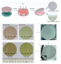
Two-dimensional semiconductors are considered key channel materials for future integrated circuits. However, the fabrication of high-quality, wafer-level two-dimensional semiconductor stacked structures with controllable layer numbers and rotation angles is quite challenging.

Recently, a research team led by Zhang Guangyu from the Institute of Physics, Chinese Academy of Sciences/Beijing National Research Center for Condensed Matter Physics developed a direct wafer bonding and debonding method to fabricate high-quality, wafer-level two-dimensional semiconductor stacks. This method can be performed in a vacuum or glove box, without the need for a transfer medium, and achieves ultra-clean surfaces/interfaces and wafer-level uniform interlayer rotations. Starting from wafer-level two-dimensional semiconductors such as monolayer molybdenum disulfide and molybdenum diselenide epitaxially grown on sapphire surfaces, this method can fabricate various homogeneous and heterogeneous stacked wafers. Characterization results from atomic force microscopy, scanning transmission electron microscopy, Raman spectroscopy, X-ray diffraction, low-energy electron diffraction, and second harmonic generation show that the fabricated two-dimensional semiconductor stacks possess high-quality, ultra-clean surfaces/interfaces and wafer-level uniform interlayer rotations.
1762957679947.png

In addition to fabricating two-dimensional semiconductor stacks, the direct bonding-debonding method can also achieve the direct transfer of various monolayer two-dimensional semiconductors from sapphire substrates to high-k dielectric substrates while preserving their intrinsic electrical properties. Compared with conventional wet transfer samples, samples transferred by bonding-debonding exhibit cleaner interfaces, resulting in field-effect devices with higher mobility, larger on-state current, and smaller threshold voltage fluctuations, demonstrating the superiority of the direct bonding method.

Direct bonding-debonding technology is fully compatible with mainstream semiconductor manufacturing processes, solving the stacking and transfer problems of intrinsic two-dimensional semiconductors, and is expected to accelerate the process of two-dimensional semiconductors from the laboratory to industrialization.


The relevant research findings were published in *Nature Electronics*. This research was supported by the National Key Research and Development Program of China, the National Natural Science Foundation of China, the China Postdoctoral Innovative Talents Support Program, and the Strategic Priority Research Program of the Chinese Academy of Sciences.

Please, Log in or Register to view URLs content!
 
Top