Chinese semiconductor thread II

tphuang

General
Staff member
Super Moderator
VIP Professional
Registered Member
I don't have links but I've been shown conversations with people in the industry (plus circumstantial evidence, such as an identical node between Kirin 9010 and 9020a which indicates a lack of equipment change) that indicate that the SSA800i was never used in production. I'm aware that this isn't ideal and you're free to distrust what I say, but I stand by that the source I got it from is credible.

As to what's actually happening with SMEE? No idea. There's some talk in other forums that SiCarrier/Huawei poached some of the SMEE people but there's been pretty much no news.
by the way, SMSC fab itself had enough ASML scanners all along, so it never made sense for SMEE scanners to be used there. It was always assumed that SMEE scanners were tested in JingCheng or one of their other 28-55nm fabs. So if your evidence is K9010 vs 9020, that's really not valid evidence.

It's entirely possible that SiCarrier had a higher goal and target all along and that they have been able to create a better product with the same supply chain that SMEE had access to. And now SMIC is finding their scanners to be sufficient to validate for 7nm process.

However, none of this indicates that SMEE scanners aren't good enough for 28-55nm nodes or that their Arf dry scanners aren't sufficient for 65-90nm node.

And by the way, many of the steps in FinFet production only need a lower spec'd scanner.
 

jx191

New Member
Registered Member
you can hook up with your insider for EUV info?
A while back rumors of EUV coming on line 3rd quarter of 2025.
There is a lot of rumors/speculation about EUV. Some ranging from production of some form in 2026, to production in 2028. Only a small circle of people know what's really going to happen in next few years with certainty.
 

Hyper

Junior Member
Registered Member
there is a lot to this that people can read and figure out.

If you look at the interconnect bandwidth and compare that to which Nvidia chips have that.

Same with memory bandwidth and compare that to HBM3/3E/4, gives you a sense of when China will get to certain node level for logic and DRAMs. EUV implication with this is quite profound.

It looks to me that they will have an Ascend-950 die in 2026Q1 that will be about 500 TFLOPS FP16 or 1 PFLOPS FP8 vs 400 TFLOPS per die for 910B die used on Ascend-910C. Ascnend-960 seems to be the 2 die version.

My guess is that Ascend-970 is the next generation die since the bandwidth is so much higher. or it is also possible that 960 could be that. From 2026Q1 to 2028Q4 is almost 3 years. Thinking that they will stick with same die over that period of time is quite uncharitable, so I think we are going to see a pretty big jump in transistor density from 2025H2 (which is when the original 950 dies are produced) to 2028H1 (which is when the 970 dies are produced)
EUV is not required for DRAM. Samsung and SK are reducing EUV layers and Micron is keeping EUV only when absolutely absolutely necessary.
 

sunnymaxi

Major
Registered Member
Like I said, I was shown conversations with field engineers, and it doesn't really matter whether you believe be or not anyway. What is demonstrably true is that between August 2023 when the Kirin 9000s launched with N+2 and June 2025 when the X90 launched, there has been no change to the process. Had there been an equipment change to the production line we would have seen some variations, but Techinsights have found identical processes in both. SSA800 is not in high volume production.
i have read your all massages..

there are few mistakes. let me clarify one by one.

everybody knows. N+1/N+2 used ASML scanner. even incoming expansion in advance nodes will use ASML machines. So if your evidence is K9010 vs 9020, that's really not valid evidence..

initially SSA800i was never meant for advanced nodes.

this machine was for mature nodes like 28nm-40nm.. even today SSA800i is in factory and continue to tap wafers but on mature nodes.. SSA800i was never tested on 7nm. who told you this ?? SMEE scanners were tested in JingCheng or one of their other 28-55nm fabs.

first SSA800i machine assembled in summer, 2021. it was the first immersion scanner in mainland China. initially machine had high defect rates got rejected.. that is true.

later on SSA800i got upgraded.

U-Precision specifically designed more precise next gen grating interferometers in 2024 for Finfet nodes include 7nm
1730244677838.png1730244631919.png

SMEE scanners are absolutely reliable for 28nm and above..
-----------------------------------------------------------------------------------------
Yulangsheng a JV between two reputed companies.. team most likely used the same supply chain that SMEE had access plus their own R&D to create the better product.. that is definitely better than original SSA800i.. otherwise SMIC wouldn't test on 7nm line..
 
Last edited:

tokenanalyst

Lieutenant General
Registered Member
Well, that's a bummer. It's seems SMEE's reputation for incompetence wasn't unfair.

How about the stuff upstream of SMEE like RSLaser, Guowang, Qier, UPrecision, etc. Do you have any idea on the performance of their components? Is SiCarrier/Yulangsheng/The Artist Formerly Known As Huawei using their stuff or do they have their own vertical?
RSLaser,Cheertech, and U-Precision from what I have read in patents and technical information they seem pretty good. Guowang there is not a lot of information but they seem to have breakthroughs.
 

sunnymaxi

Major
Registered Member
Well, that's a bummer. It's seems SMEE's reputation for incompetence wasn't unfair.

How about the stuff upstream of SMEE like RSLaser, Guowang, Qier, UPrecision, etc. Do you have any idea on the performance of their components? Is SiCarrier/Yulangsheng/The Artist Formerly Known As Huawei using their stuff or do they have their own vertical?
we need results.. whether its from SMEE or Yulangsheng.

Sicarrier and Huawei had to involved when they saw incompetency from SMEE.. the main reason why they created JV. Yulangsheng most likely design DUVi with the same supply chain that SMEE had access to plus their own output.

U-Precision and RSLaser technical information are pretty good.. these are Beijing based firms.

@LanceD23 ..
 

tamsen_ikard

Senior Member
Registered Member
i have read your all massages..

there are few mistakes. let me clarify one by one.

everybody knows. N+1/N+2 used ASML scanner. even incoming expansion in advance nodes will use ASML machines. So if your evidence is K9010 vs 9020, that's really not valid evidence..

initially SSA800i was never meant for advanced nodes.

this machine was for mature nodes like 28nm-40nm.. even today SSA800i is in factory and continue to tap wafers but on mature nodes.. SSA800i was never tested on 7nm. who told you this ?? SMEE scanners were tested in JingCheng or one of their other 28-55nm fabs.

first SSA800i machine assembled in summer, 2021. it was the first immersion scanner in mainland China. initially machine had high defect rates got rejected.. that is true.

later on SSA800i got upgraded.

U-Precision specifically designed more precise next gen grating interferometers in 2024 for Finfet nodes include 7nm
View attachment 160966View attachment 160967

SMEE scanners are absolutely reliable for 28nm and above..
-----------------------------------------------------------------------------------------
Yulangsheng a JV between two reputed companies.. team most likely used the same supply chain that SMEE had access plus their own R&D to create the better product.. that is definitely better than original SSA800i.. otherwise SMIC wouldn't test on 7nm line..
Do we have any production microchip using china's domestic lithography machine in 28nm?

So far I have only seen rumours of testing but no production execution.

Same thing with EUV. I think we are being overly optimistic. I think China will not be able to get EUV and make actual production chip in the next 5 years when they are so far behind in DUV lithography.
 

tphuang

General
Staff member
Super Moderator
VIP Professional
Registered Member
EUV is not required for DRAM. Samsung and SK are reducing EUV layers and Micron is keeping EUV only when absolutely absolutely necessary.
"reducing EUV layers" - so they still need EUV. CXMT is likely to get to D1a without EUV, but I would imagine D1b and D1c would both use it.

And similarly, if you want to do Serdes chips with higher transmission, you need more advanced nodes like 3-5nm.

So yes, they would need EUV producing chips in HVM by 2027 for some of these products to be productive.

And the fact that Huawei can give a timeline is an indication that it sees a clear road path from where things are right now.

Do we have any production microchip using china's domestic lithography machine in 28nm?

So far I have only seen rumours of testing but no production execution.

Same thing with EUV. I think we are being overly optimistic. I think China will not be able to get EUV and make actual production chip in the next 5 years when they are so far behind in DUV lithography.
DUV and EUV are not the same stack.

As for whether any chips have been produced with domestic lithography machine @ 28nm. I would think so, but I think the better question is in HVM. I would think likely in HVM, but we don't know for sure. And I don't think it's all that important to know, because they have access to DUVi scanners for 28nm.

And if the Yulangsheng scanner is being used for 7nm, then it should be close to validating for less advanced nodes. After all, how does HW build so many new fabs without lithography machines?

People are overly concerned about things that are not that important.
 

snake070

New Member
Registered Member
you can hook up with your insider for EUV info?
A while back rumors of EUV coming on line 3rd quarter of 2025.
Fake news

科研项目​

( 1 ) 高平均功率激光等离子体极紫外光刻光源关键技术及相关基础研究, 参与, 国家任务, 2023-08--2028-08
( 2 ) 万瓦级高重频窄脉宽CO2激光器, 参与, 中国科学院计划, 2023-08--2028-08
( 3 ) 2023曙光计划-极紫外光刻光源高功率CO2驱动激光光束控制, 负责人, 研究所自主部署, 2023-07--2026-06
( 4 ) 极紫外光刻光源高功率驱动激光光斑的高精度快范围快响应检测技术研究, 负责人, 国家任务, 2022-01--2024-12
( 5 ) 面向复杂环境的多体制高功率激光器通用散热与热控技术研究, 参与, 国家任务, 2019-08--2024-08

科研项目​

( 1 ) XXX项目研制, 参与, 其他, 2024-01--2025-12
( 2 ) EUV光源舱体诊断, 参与, 中国科学院计划, 2023-10--2027-07
( 3 ) 浸没式曝光光源研制与小批量产品生产能力建设, 参与, 国家任务, 2016-01--2022-12
( 4 ) ArF 光源产品整机设计、集成制造与试验, 参与, 国家任务, 2013-01--2021-12
( 5 ) 激光放电腔研发, 参与, 国家任务, 2013-01--2021-12
( 6 ) 产品可靠性寿命研究, 参与, 国家任务, 2013-01--2021-12

研究方向:

高端光刻机技术,EUV光刻光源,光学精密检测技术。

承担项目:

作为负责人,承担中国科学院A类先导专项项目、国家科技重大专项(02 专项)任务、科技部国际科技合作课题、国家自然科学基金面上项目、国家重大科研仪器研制任务、上海市科委重点项目等 10 余项科研任务。

学术成果:

作为中国科学院A类先导专项副总设计师和项目负责人,开展激光等离子体光源的攻关;研发的偏振检测技术为光刻机偏振照明系统、投影物镜验证提供了关键检测手段,为研发光刻机照明系统和投影物镜提供了重要技术支撑;研发的手持式眼底照相机已上市销售。在Optics express、Optics Communicationns、Scientific reports等国际、国内一流光学期刊上发表学术论文50余篇,获发明专利授权20余项。
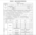
( 14 ) 系统设计、集成与测试, 负责人, 中国科学院计划, 2023-10--2027-12


本项目针对光源系统设计、系统集成与测试方面的需求开展研究,在光源建模、系统实验平台、 高精度工装、系统在线测试与性能评估、光源舱体诊断等方面取得突破。预期成果如下:
1、 在系统设计阶段完成光源系统层面的定义和指标拆解,进行系统硬件和软件设计,指导整 机集成关键参数优化设置的同时,探究提高转换效率的新方案。
2、 在系统集成阶段建立系统实验平台和集成工装,实现开环下激光精准打靶,以获得最佳的 能量输出,为实现专项的整机性能指标提供集成保障。
3、 在系统集成过程中,开展光源系统在线测试工作,指导光源整机集成调试,以实现光源系统 开环状态下的精准打靶;同时研究高精度、在线、无损的污染气体快速诊断技术。
4、 在光源整机集成调试后,开展光源光谱、功率、近场/远场分布、污染物等检测,实现光源 集成调试后系统性能的全面评估。
完成基于初样一代舱阶段 光源舱分系统的第一轮系统集成,开展调试
EUV集成.png
 

sunnymaxi

Major
Registered Member
Do we have any production microchip using china's domestic lithography machine in 28nm?

So far I have only seen rumours of testing but no production execution.

Same thing with EUV. I think we are being overly optimistic. I think China will not be able to get EUV and make actual production chip in the next 5 years when they are so far behind in DUV lithography.
tphuang just replied you..

we have volume production in 28nm chips using domestic machine. but the issue is, people only care about advanced nodes.

just yesterday news came, domestic DUVi being tested in 7nm advanced node at SMIC.

EUV program initiated way before DUVi project. and both DUV and EUV are not the same stack.
 
Top