Chinese semiconductor thread II

huemens

Junior Member
Registered Member

Synopsys Falls Most in Three Decades as Trade War Hampers Sales​

Please, Log in or Register to view URLs content!
Shares of chip-design software maker Synopsys Inc. plunged the most in more than three decades after the company warned that US export restrictions are contributing to a slowdown in China, the largest market for semiconductors.
As part of the company’s quarterly report on Tuesday, Chief Executive Officer Sassine Ghazi said that a push to develop its own intellectual property isn’t achieving the desired results — partly because of the China challenges. Ghazi said he would be refocusing resources on other areas and is reducing the company’s headcount by about 10%.
“Our results were primarily impacted by underperformance in the IP business as we had the expectation of deals that did not materialize, driven largely by the following three factors: one, new export restrictions disrupted design starts in China, compounding China weakness; two, challenges at a major foundry customer are also having a sizable impact on the year,” Ghazi said on a call with analysts. “And finally, we made certain road map and resource decisions that did not yield their intended results.”
The shares fell as much as 34% after markets opened in New York on Wednesday, their biggest intraday decline since 1992. They had been up 25% this year through Tuesday’s close.
 

tokenanalyst

Brigadier
Registered Member
From The Chinese Academy of Science, A recap on the work on the Immersion Lithography Machine.

Pre export controls:


The development of lithography machine worktables exemplifies the synergy between independent innovation and technological pre-research. In 2001, ASML launched the world’s first dual-worktable system. By 2003, Tsinghua University’s IC Equipment Team, anticipating generational leaps, filed China’s first dual-worktable patent, deliberately skipping the single-worktable phase. Recognizing planar motors’ potential, they began exploratory research in 2005 and published China’s first academic paper on the topic in 2006. This laid the groundwork for their 2008 scaled-down prototype, which, though still using linear motors and air bearings, provided essential validation for future independent innovation.

When China’s National Key R&D Program for IC manufacturing launched in 2009, ASML had already moved to magnetically levitated planar motors, far outpacing older architectures. Continuing down the conventional path would have meant immediate obsolescence. Despite daunting theoretical and engineering challenges, the team chose the planar motor route to break the “develop-and-lag” cycle. Through innovation, including air/magnetic levitation architecture, redundant eight-motor drive, zero-phase error tracking, and ultra-stable dynamic balancing, they developed China’s first dual-worktable planar motor prototype, establishing a new technological baseline.

The measurement system’s evolution also reflects strategic foresight. In 2009, ASML adopted plane grating displacement measurem, a leap beyond China’s entrenched laser interferometry. The Tsinghua team initiated pre-research in 2010 and by 2011 built China’s first plane grating interferometer, proposing a zero-difference fringe locking solution to correct distortion in large-scale grating fabrication. This groundwork enabled their 2017 national project breakthroughs: heterodyne interferometry, meter-level ultra-precision grating manufacturing, picometer-accuracy posture algorithms, and robust system integration achieving sub-nanometer, high-dynamic measurement capability.

Post Export Controls:

Breakthroughs in dual worktables and plane gratings have yielded transformative results. China’s lithography systems now match ASML’s architectural sophistication with full IP ownership, a structural leap. These wins validate that during technological transitions, only forward-looking planning and sustained pre-research can overcome path dependence.
Strategic foresight initiates breakthroughs; independent innovation breaks barriers; long-term investment ensures results. This triad, reinforced by courage forms a replicable paradigm for high-end equipment, laying the foundation for full lithography ecosystem independence.

Independent innovation faces dual constraints: fragmented markets hinder demand aggregation and ROI on foundational materials/components; foreign firms enforce patent walls and supply blockades on precision processes. This traps domestic players in a vicious cycle, high R&D risk, low market return, stalling foundational capability growth despite urgent strategic needs.

To counter this, national projects established a demand-aggregation and risk-sharing mechanism — integrating fragmented needs and channeling special funds to foster industry-wide collaboration.
Within this, the Tsinghua-Huazhuo Joint Team working with upstream and downstream partners targeted three critical bottlenecks: ceramics, suction cups, and magnet arrays turning systemic weakness into coordinated national progress.

High-performance cordierite ceramics now standard in advanced lithography stages were long monopolized by Japan. Under embargo pressure, the Joint Team collaborated with domestic firms to master raw material synthesis, defect-free sintering, and precision optical machining. The result: China now ranks among the few nations capable of mass-producing ultra-low expansion ceramics dramatically improving thermal stability and stage performance.

Ultra-thin suction cups requiring micron-level flatness, hardness, and thermal stability lagged in domestic capability. The Joint Team partnered with material and machining firms to innovate: controllable conductivity materials, high-precision bump fabrication, and ultra-smooth polishing. The outcome: high-performance domestic suction cups that reduce import reliance, enable repair of foreign systems, and strengthen China’s IC equipment autonomy.

Planar motor magnet arrays, long protected as proprietary foreign know-how posed challenges in assembly precision, field uniformity, and large-surface machining. The Joint Team responded with an intelligent error-correction tooling system, periodic field consistency control, precision protective layer processing, and safe high-yield assembly methods. The result: high-performance magnet arrays that significantly boost stage speed, accuracy, and reliability.

These foundational wins have not only advanced lithography stage R&D but also strengthened the entire supply chain. They prove that under blockade, sustained investment, interdisciplinary collaboration, and national coordination can achieve self-reliance offering a scalable model for other high-end equipment sectors facing similar constraints.

The Joint Team established an efficient “four-in-one” collaboration system linking suppliers, R&D consortia, OEMs, and end-users coordinated through national projects. This enabled end-to-end innovation, from basic materials to integrated machines, transforming fragmented efforts into synchronized national capability.

During glass-ceramic mirror localization, foreign delivery delays prompted the team to simplify design and mobilize four key domestic enterprises including state-owned heavyweights under national project coordination. Three succeeded in mastering core technologies, achieving independent control a clear demonstration of how national projects integrate industrial capacity where markets alone cannot.


For specialized planar motor coils low-volume, no existing suppliers the team adopted a “process-driven” model: developing the full manufacturing process and custom equipment for partner firms. This cultivated a qualified domestic supplier offering a replicable pathway for localizing other niche, high-precision components.

User insight proved decisive. When the team initially favored dual-frequency laser interferometry, end-users drawing on real fab needs insisted on adopting planar grating technology.
Heeding this advice avoided costly iteration and directly enabled China’s leapfrog advancement underscoring the value of embedding user feedback in R&D.

The “large-scale production line verification” mechanism accelerated maturity. For a lithography stage, close collaboration with OEMs and fab engineers resolved hundreds of issues boosting equipment uptime from under 50% to over 90%, nearing global benchmarks. This iterative, application-driven approach drastically shortened the lab-to-fab timeline.

These cases show lithography breakthroughs stem not just from technology, but from the national project’s coordination mechanism — achieving three critical shifts: 1) From academic R&D to demand-driven innovation, 2) From isolated firms to industry-wide collaboration, 3) From slow lab validation to rapid production-line iteration. This model offers vital lessons for China’s high-end equipment self-reliance.

Lithography stage progress rests on three pillars: long-term national funding, evolving industry-academia-research collaboration, and strategic alignment with national priorities. Together, they form a uniquely Chinese innovation model purpose-built to achieve technological sovereignty in critical, high-barrier domains.​

----------------------------

1- This dismiss claims that is just SMEE working in the lithography machines.

2- As we predicted here China is not just building a "lithography machine" but an entire supply chain for building all kind of lithography machines. Materials, ultra high precision numerical machines and components.

3- Fabs like SMIC, YMTC, CXMT and even HHGrace are not just working in the validation and testing of these machines. They are active participants in the development of these machines, for example when they suggested to the team instead of using dual interferometry to develop Planar Grating Interferometers base on their experience.

4- As I said multiple times here, China has purely almost 100% domestic fabs since 2021-2022 to test and validated equipment, materials and components. Creating a less risky path for domestic fabs to adopt domestic made tools.

5-As we said here, China is using components made in this domestic supply chain to repair and maintain sanctioned lithography machines, one of the reasons why SMIC has been keeping operating all this time.
 

sangye

Junior Member
Registered Member

Jingcun's subsidiary, Miaocun Technology, releases its new blockbuster QLC NAND UFS 2.2 storage​

As smart devices continue to pursue high performance and large capacity, QLC NAND UFS memory is becoming a focus of industry attention. Compared to traditional TLC architecture, QLC offers higher storage density and a more cost-effective price, but it also places higher demands on storage controllers and firmware.
821527ac78242db8fa8d87071f9d28de.png

Building on its long-term experience and R&D investment in controller chip technology, Jingcun Technology, a subsidiary of Jingcun, has launched its new QLC NAND UFS 2.2 storage product . Notably, Miaocun Technology pioneered the release of UFS controllers and modules at the end of last year. This new product launch aims to provide the end market with a storage solution that combines high performance with high cost-effectiveness.

Relying on independently developed controller technology and continuously optimized firmware solutions, Miaocun Technology's QLC NAND UFS 2.2 memory achieves a precise balance between capacity and performance, with excellent performance and stable operation capabilities. It can better unleash the potential of QLC NAND and meet the needs of terminal devices in diverse scenarios such as system startup, application loading, and interactive response.

MiCun Technology's QLC NAND UFS 2.2 Memory Core Advantages
01 Self-developed controller + customized firmware optimization
Equipped with the self-developed UFS controller chip ATM102, it conducts in-depth analysis of QLC NAND characteristics and optimizes the firmware design by combining software and hardware.

Customized firmware can effectively improve QLC NAND's read and write efficiency, lifespan, and energy consumption, ensuring product stability and reliability.
02 Excellent performance, far exceeding eMMC
The comprehensive performance of QLC NAND UFS 2.2 memory is about three times that of eMMC, the price is close to that of eMMC, and it is superior to TLC UFS 2.2 in some indicators.​
  • Sequential read >900MB/s
  • Sequential write speed >800MB/s
  • Random read and write speeds can exceed 500MB/s, and some indicators are even better than TLC NAND UFS 2.2 products.
03 Flexible capacity selection
Currently, the products cover three capacity segments: 128GB, 256GB, and 512GB. In the future, we will further launch 1TB and 2TB ultra-large capacity products to meet the diverse needs from mid-range to high-end devices.
04 Wide range of application scenarios
The product is suitable for consumer electronic terminals such as smartphones and tablets, and is compatible with mainstream control platforms, providing OEM manufacturers with an ideal storage solution with large capacity, high cost performance and high performance.

Please, Log in or Register to view URLs content!
for those of you, like me, that were left scratching their heads wondering why a flash memory manufacturer would release a product carrying a lower version number of the UFS standard currently in use. I found a very informative article written by Nothing (the phone company).
Please, Log in or Register to view URLs content!


UFS 2.2 specifications was released half a year after UFS 3.1, something this article doesn't mention, so the debate is about big number vs small number rather than older standard vs newer one.
 

tokenanalyst

Brigadier
Registered Member

SMIC, China Resources Microelectronics and others have stepped up efforts in chip manufacturing.​

SMIC's acquisition of 49% stake in SMIC North Technology has made new progress

On September 9, SMIC disclosed a plan to acquire a 49% minority stake in its subsidiary SMIC North Integrated Circuit Manufacturing (Beijing) Co., Ltd. (hereinafter referred to as "SMIC North") by issuing shares. SMIC plans to acquire a 49% stake in SMIC North America through a full issuance of new shares to minority shareholders. Upon completion of the transaction, SMIC's stake in SMIC North America will increase from 51% to 100%, making SMIC North America a wholly-owned subsidiary of SMIC. The price of SMIC's additional issuance to acquire SMIC North has reached 74.20 yuan per share, but because the audit and evaluation of the target assets have not been completed, the final overall transaction pricing is yet to be determined.

According to information, SMIC North focuses on 12-inch wafer foundry and has the mass production capabilities of multiple process platforms such as logic circuits, low-power logic circuits, high-voltage drives, embedded non-volatile storage, mixed signal/RF, image sensors, etc., and can provide customers with integrated circuit wafer foundry and supporting services in different terminal application fields such as smartphones, computers and tablets, consumer electronics, Internet and wearables, industry and automobiles. SMIC pointed out that "this transaction will help further improve the asset quality of the listed company, enhance business synergy, and promote long-term development."

Aosong Semiconductor's 8-inch MEMS specialty chip IDM industrial base project has been put into production

On September 9, the commissioning ceremony of Aosong Semiconductor's 8-inch MEMS specialty chip IDM industrial base project was held in Chongqing. According to the information, the Aosun Semiconductor project is located in the Western (Chongqing) Science City. It is Chongqing's first 8-inch MEMS specialty chip full industrial chain project. The project has a planned total investment of 3.5 billion yuan, including the construction of an 8-inch MEMS specialty sensor chip mass production line, an 8-inch MEMS specialty wafer rapid R&D line, an intelligent sensor innovation R&D center, an automotive-grade sensor reliability testing center, an industry-university-research research center and an Aosun Semiconductor R&D office building.

The project is expected to reach full production in December 2026. By then, it will provide strong support for the core components of the supply chain for strategic pillar industries and strategic emerging industries in the Chengdu-Chongqing Economic Circle, including automobiles, rail transit, biomedicine and health, smart home appliances, intelligent robotics, high-end equipment manufacturing, precision instruments and equipment, and smart grids.

Rongxin Semiconductor responds to the progress of Ningbo 12-inch project

On September 8, Rongxin Semiconductor Co., Ltd. (hereinafter referred to as "Rongxin Semiconductor") issued a statement in response, stating that since July 2024, Dr. Yang Shining has served as the chairman of the company's technical expert committee to guide related work; the company's Ningbo project is progressing as planned. According to information, Rongxin Semiconductor was established in April 2021 and is headquartered in Ningbo City, Zhejiang Province. It focuses on the manufacturing of 12-inch integrated circuits with mature processes (28 to 180 nanometers) and special processes, and focuses on CIS (image sensor chips), TDDI (touch and display driver chips), BCD (power management chips), display driver chips, new storage and other mixed digital and analog and analog integrated circuit products. The downstream application scenarios cover industrial control, consumer electronics, digital home, mobile communications and automotive electronics.

Rongxin Semiconductor currently has two major production bases in Huai'an, Jiangsu, and Ningbo, Zhejiang. The Huai'an production line is expected to enter mass production in 2022. Construction of the Ningbo 12-inch integrated circuit chip production line began in April this year with a total investment of 16 billion yuan. The company plans to achieve a monthly production capacity of 35,000 wafers, with the goal of achieving a monthly production capacity of 200,000 12-inch wafers by 2030, creating a comprehensive integrated circuit manufacturing platform with annual sales revenue exceeding 30 billion yuan.​
 

tokenanalyst

Brigadier
Registered Member

China Resources Microelectronics' Chongqing 12-inch project achieved its planned goals ahead of schedule

On September 5, China Resources Microelectronics held a special meeting on the product volume increase of its 12-inch power semiconductor wafer production line at its Chongqing campus. At the meeting, it was announced that the project had achieved its monthly output target of 30,000 wafers in August 2025, one and a half years ahead of the original planned node. This important progress marks that China Resources Microelectronics has successfully built a 12-inch automotive-grade power semiconductor wafer manufacturing platform with outstanding domestic competitive advantages in Chongqing, achieving independent control of high-end power chip technology and reliable supply of the entire manufacturing process.

It is reported that the Chongqing 12-inch project is committed to building a world-class high-end power device wafer production line: the proportion of new industry-leading machines reaches 95%; it has a global top-brand overhead crane system and automated production scheduling system, matched with automated three-dimensional warehousing to create an industry-leading unmanned factory; the product layout is benchmarked against the world's latest process generations, and core technology platforms such as SGT G6, SJ G4, and IGBT G7 fully serve high-end application fields such as automobiles, AI, and computing centers; it is equipped with a 70,000-square-meter automotive-grade power module packaging and testing base to provide one-stop IDM efficient services; establish a full-process automotive-grade quality system, equipped with an investment of over 200 million yuan, an area of over 4,000 square meters, and more than 30 CNAS-approved automotive-grade laboratories, and the product online yield is stable at above 99.65%.

Chongqing's 6-inch power semiconductor plant and supporting facilities are about to be put into use

Chongqing Xinling Microelectronics Co., Ltd. (hereinafter referred to as "Chongqing Xinling Micro") has made steady progress in its 6-inch power semiconductor plant and supporting facilities project, with civil construction for all buildings approximately 90% complete. The equipment for the pure water and wastewater stations has been fully installed and is currently undergoing commissioning. The bulk gas station was fully installed in mid-August. The entire supporting system is expected to be operational in October of this year, providing critical support for smooth product production. According to information, Chongqing Xinlingwei was established in July 2022 and was jointly invested by Ningbo Daxin Semiconductor Co., Ltd. and Fuling District New City District Development (Group) Co., Ltd. It is a high-tech enterprise focusing on power semiconductor chip manufacturing with a total investment of approximately 2 billion yuan.

In June of this year, Chongqing Xinling Microelectronics achieved full production of the backside of its chips and has already reached small-batch production. Currently, frontside production equipment is being installed, and the frontside process is expected to be fully operational this year, completing the entire production line. Once the project reaches full production, it will ultimately achieve an annual output of 1.2 million 6-inch wafers, significantly alleviating the urgent domestic demand for high-end power semiconductor chips.

In the next step, the company will rely on Chongqing's new energy vehicle industry chain, focus on the new energy vehicle market, and strive to build a first-class domestic power semiconductor chip manufacturing base, fill the gap in Fuling District in the power semiconductor industry, and help the regional advanced manufacturing industry achieve high-quality development.


Please, Log in or Register to view URLs content!
 

tokenanalyst

Brigadier
Registered Member

JCS-3000 Spectroradiometer | Redefining color measurement, unlocking new horizons in display​

With the accelerated iterative innovation of new display technologies such as OLED, Mini-LED, and Micro-LED and the continuous upgrading of industry standards, in order to meet the diversified display measurement needs, Jingce Electronics' subsidiary Jingyi Micro Instruments, relying on its leading advantages in the field of precision optical testing, deeply integrates color science and measurement technology, and independently develops and launches the JCS-3000 spectroradiometer (spectrometer). It integrates circuit optimization processing, optoelectronic testing systems and other capabilities to help customers achieve accurate measurement, reduce costs and increase efficiency, and improve yield.

1757527845840.png

Please, Log in or Register to view URLs content!
 

tokenanalyst

Brigadier
Registered Member

Suzhou Institute of Nanotechnology has made progress in β-Ga₂O₃ vertical power devices​


As a strategic advanced electronic material, the ultra-wide bandgap ( UWBG ) gallium oxide ( β- Ga2O3 ) is rapidly emerging as a disruptive force in power electronics in the post-Moore era, thanks to its exceptionally high breakdown field strength of 8 MV/cm and unique advantages in large-scale melt growth. Vertically structured power electronics , through optimized longitudinal voltage-resistant layer design, achieve both high withstand voltages of 10,000 volts ( 10 kV) and high current capabilities of kiloamperes (kA) per unit chip area. This perfectly meets the urgent demands for ultra-high power density, high efficiency, and miniaturization in smart grids, new energy vehicles, industrial motor drives, data center power supplies, and renewable energy (photovoltaic and wind) converters.

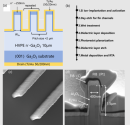
Recently, the Nanofabrication Platform of Suzhou Institute of Nano-Tech and Nano-Bionics, Chinese Academy of Sciences, has developed a new nanostructured ...Two major breakthroughs have been achieved in the field of β-Ga2O3 power devices: First, a multi - fin channel ohmic contact anode β - Ga2O3 diode (MFCD) fabricated using a nanofabrication platform-developed process achieved a kilovolt-level breakdown voltage with ultra- low leakage . Furthermore, a high-performance enhancement-mode vertical β- Ga2O3 multi -fin transistor was developed , achieving a record-breaking low specific on-resistance of 4.3 mΩ·cm² . Both achievements offer novel solutions for high-temperature and high-voltage applications .

1757529279539.png
Figure 1( a) Schematic diagram of a multi-fin channel β- Ga2O3 diode , (b) key process steps of the device , ( c) scanning electron microscope (SEM) image after fin dry etching , (d) SEM cross-sectional image of a diode with a fin width of 400 nm .
.
The device replaces the traditional Schottky structure with an original ohmic contact anode design, and combines the sidewall self-depletion effect caused by the submicron fin channel to successfully solve the problem of leakage runaway in wide bandgap semiconductor devices under high electric fields. Without any field plate or passivation layer assistance, 0.1μm narrow fin device showed 1148V breakdown voltage, reverse leakage current is maintained at 1μA/cm² commercial level, and at 150There is no performance degradation in high temperature environment. The introduction of ohmic contact reduces the specific on-resistance to 7mΩ·cm², which is 35% lower than that of similar trench Schottky diodes. This breakthrough can provide a new solution for high-voltage scenarios such as photovoltaic inverters and electric vehicle fast charging piles .​

Please, Log in or Register to view URLs content!
 

tokenanalyst

Brigadier
Registered Member

Shanghai Xinyang: Photoresist sales increase, 2025 revenue target exceeds 1.7 billion​


Shanghai Xinyang Photoresist Sales Improve, 2025 Revenue Target Cleared: On September 10th, Shanghai Xinyang released a record of its investor relations activities. Currently, the company's various KrF photoresist products are in mass production, and overall photoresist sales continue to grow. ArF immersion photoresist has also received sales orders.

As of the first half of 2025, the company will serve as the baseline for 56 12-inch and 23 8-inch production lines operating in China, accounting for over 70% and 60% of the total integrated circuit production lines, respectively.
According to the performance assessment targets of the equity incentive plan, the company's semiconductor industry revenue is expected to be no less than 1.3 billion yuan in 2025, and consolidated revenue is expected to be no less than 1.7 billion yuan. The company will strive to achieve these goals.

Please, Log in or Register to view URLs content!
 

tokenanalyst

Brigadier
Registered Member

A world first! Deke Micro releases millimeter-wave based isolated communication technology.​


Recently, Shenzhen high-tech enterprise - Decr Microelectronics (Shenzhen) Co., Ltd. (hereinafter referred to as "Deke Micro") officially released the world's first digital isolation chip based on millimeter wave ultra-short distance communication. The isolated communication rate can reach up to 5Gbps with lossless transmission under a power withstand voltage of over 10,000 volts, setting off another "technological revolution" in isolated communication.

1757533888752.png

Millimeter-wave wireless isolation chips drive new application possibilities

DeKe Micro has creatively applied ultra-short-range millimeter waves to the field of isolated communications, cleverly using millimeter-wave on-chip antennas to conduct coupled communications within the chip package through insulating media, naturally achieving a 10,000-volt withstand voltage. It has core advantages such as 5GHz switching frequency, 20ps-level latency and 6.25Gbps bandwidth, breaking the structural contradiction of "it is difficult to achieve high frequency, high voltage resistance and low latency at the same time". It does not rely on semiconductor processes and technologies, has a simpler package, and has a more competitive system cost.

Millimeter-wave technology, previously primarily used in radar, communications, and sensing, has been introduced by Deke Micro for the first time into a digital isolation chip architecture. This technology supports universal insulation materials and ultra-wide temperature environments, and boasts multi-directional integration capabilities and millimeter-scale antenna-coupled communication, bringing new application possibilities to a wide range of electronic systems. For the entire electronics industry, this represents a complete transformation, from underlying connectivity architecture to system form factors.

As a Shenzhen-based high-tech enterprise and a specialized, innovative enterprise, Deke Micro, leveraging its groundbreaking technologies, has established a robust patent portfolio in major global markets, with 238 applications and 117 authorizations. Deke Micro focuses on the development of millimeter-wave wireless chips and system-level solutions, with comprehensive intellectual property rights. Its products have been commercialized on a large scale in areas such as LED displays and industrial control, leading global technological innovation with Chinese core intelligence.

At present, Deke's micro-millimeter wave wireless isolation chip has passed the testing and verification of many leading companies in the industry chain, and is accelerating into the large-scale mass production stage. In the future, it will be widely used in automotive-grade electronics, industrial modules, consumer terminals and other fields.​

Please, Log in or Register to view URLs content!
 
Top