You are using an out of date browser. It may not display this or other websites correctly.
You should upgrade or use an alternative browser.
You should upgrade or use an alternative browser.
Chinese semiconductor thread II
- Thread starter vincent
- Start date
Nanxin Technology launches China's first domestically produced supply chain vertically integrated process high-side switch
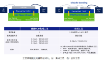
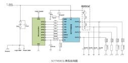
Nanxin Technology (stock code: 688484) officially released the second-generation automotive-grade high-side switch (HSD) SC77450CQ. Leveraging a domestically developed vertical channel BCD integration process and a fully domestically produced packaging and testing supply chain, the SC77450CQ integrates MOS and controllers on a single wafer with an N-type substrate , offering customers a more convenient system development experience. Breaking the monopoly of overseas technology, the SC77450CQ is the first domestically produced high-side switch to utilize a vertically integrated process with a fully domestically produced supply chain .
The Boxin microelectronics packaging project with a monthly output of 200 million chips has officially started production
Boxin Microelectronics (Tianjin) Co., Ltd. (hereinafter referred to as "Boxin Microelectronics") officially started production in the Microelectronics Innovation Industrial Park of Tianjin Economic and Technological Development Zone. After the project reaches full production, the monthly packaging chip capacity is expected to be more than 200 million pieces, and the annual revenue will reach more than 200 million yuan.

According to reports, Boxin Microelectronics primarily manufactures two packaging types: DFN (Dual Flat No-Lead) and QFN (Quad Flat No-Lead). Their primary packaging products are power protection chips. In addition to increasing production capacity for existing products, Boxin Microelectronics will also add a flip chip advanced packaging prototype line, power SiC (silicon carbide) and GaN (gallium nitride) chip packaging, as well as RF modules and audio amplifier IC modules, gradually expanding from miniaturized packaging to advanced packaging.
According to information, Boxin Microelectronics was established in 2022 and registered by the Institute of Microelectronics of the Chinese Academy of Sciences. It is a company focusing on semiconductor integrated circuit packaging and testing.
According to information, Boxin Microelectronics was established in 2022 and registered by the Institute of Microelectronics of the Chinese Academy of Sciences. It is a company focusing on semiconductor integrated circuit packaging and testing.
Hefei Xinyihua's domestically produced AMHS has been moved into the third-generation semiconductor production line
According to "Hefei Xinyihua", Hefei Xinyihua Intelligent Machinery Co., Ltd. (hereinafter referred to as "Xinyihuazhi") completed the relocation of the first batch of domestically produced AMHS equipment in a third-generation semiconductor wafer factory.
This project is the customer group's second purchase and cooperation after the first domestic 8-inch front-end process Fully Auto AMHS localization project, and it also sets a milestone in the domestic breakthrough of AMHS localization in the third-generation semiconductor field in China.

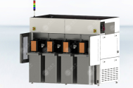

This delivery demonstrates Xinyi Huazhi's technical strength and efficient delivery capabilities in the semiconductor AMHS field. Its system, through its independently developed dynamic scheduling algorithms and clean handling technology, provides critical support for China's high-end wafer manufacturing. This project marks a new phase in the strategic collaboration between the two parties. Xinyi Huazhi will accelerate system integration and commissioning to ensure the production line is put into production on schedule, contributing to independent innovation and high-quality development in the integrated circuit industry.
This project is the customer group's second purchase and cooperation after the first domestic 8-inch front-end process Fully Auto AMHS localization project, and it also sets a milestone in the domestic breakthrough of AMHS localization in the third-generation semiconductor field in China.


This delivery demonstrates Xinyi Huazhi's technical strength and efficient delivery capabilities in the semiconductor AMHS field. Its system, through its independently developed dynamic scheduling algorithms and clean handling technology, provides critical support for China's high-end wafer manufacturing. This project marks a new phase in the strategic collaboration between the two parties. Xinyi Huazhi will accelerate system integration and commissioning to ensure the production line is put into production on schedule, contributing to independent innovation and high-quality development in the integrated circuit industry.
Aberration model in extreme ultraviolet lithography for device reliability
Abstract
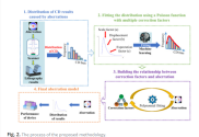
As one of the most critical processes in the manufacturing of micro-nano devices, the quality of the lithography results affects the reliability of devices and the realization of circuit functions directly. Moreover, the manufacturing of gate-all-around (GAA) devices must rely on the most advanced extreme ultraviolet lithography (EUVL). However, aberrations in the EUV lithography system have a significant and non-negligible impact on the lithography results. In order to reflect the relationship between the aberrations and the critical dimension (CD) of the lithography results intuitively and further estimate the changes in device performance, this paper proposes an analytical aberration model for device reliability. In an attempt to reduce the incidence of large aberrations in EUVL by introducing a Poisson distribution function with multiple correction factors, the distribution of the CD variation is obtained under the influence of aberrations. Then, the functional relationships between the magnitude of the aberrations and each correction factor are obtained by curve fitting. By integrating the above results, an analytical model depicting the relationship between the magnitude of aberrations and the distribution of the CD variation is ultimately established. Based on this model, the distribution of lithography results under various aberrations can be clearly visualized, and then the changes in device performance and even the functions of the entire circuit can be estimated. For example, when the root mean square (RMS) value of the aberration is restricted from 50mλ to 40mλ, the change in the saturation current of the GAA device will decrease by 30.9%. This model can help designers understand the basic process capabilities and the realization of functions before device manufacturing, and then optimize at the design stage to avoid excessive performance losses caused by the process in the early stage of design.
Topological homeomorphism extends orthogonal polynomials to arc-shaped apertures for an extremely-low aberration system
Abstract
Orthogonal polynomials are indispensable in optical engineering for aberration control and surface machining, yet their application in non-circular apertures remains a persistent challenge. While Zernike polynomials effectively decompose wavefront errors into physically meaningful terms within circular domains, their orthogonality fails in arc-shaped apertures—a critical geometry for extreme ultraviolet lithography (EUVL) systems employing curved fields to avoid light obscuration. This breakdown severely limits high-precision surface correction and aberration control in freeform optics. To address the breakdown of orthogonality for traditional orthogonal polynomials in irregular domains, this study employs the principle of topological homeomorphic transformation to establish a bidirectional mapping function between irregular and regular regions, thereby extending the orthogonality domain of conventional orthogonal polynomials. Taking the irregular effective aperture in EUVL objective lens systems as an example, we derived arc-shaped Legendre orthogonal polynomials (ALOP) and verified their advantages over traditional polynomials through two distinct application scenarios. The introduction of ALOP into the optical design of the six-mirror system has led to a further enhancement of the system’s imaging quality, and the wavefront aberration root mean square (RMS) has been optimized from the original 0.148 nm to 0.098 nm. In the context of surface figure refinement applications, we simultaneously established a deterministic mapping between the ALOP parameters of individual mirror surfaces and optical aberrations. This mapping enabled the reduction of the full-field wavefront aberration RMS in the projection optical system from 1.77 nm to 1.05 nm via single-mirror refinement, achieving a refinement efficiency exceeding 40. Furthermore, the methodology established in this study—linking irregular domains with regular domains through topological homeomorphic transformation—addresses the challenges posed by non-conventional geometries and pupils in advanced optical systems, and provides fresh perspectives for the design and fabrication of future high-precision, highly complex optical systems.
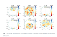
The influence of Nonlinear Overlay Error Correction on Critical Dimension
Shanghai Microelectronics Equipment (Group)
Abstract
The critical dimension uniformity (CDU) and the overlay accuracy are key index that determines the performance of thinfilm transistors (TFT). The exposure fading caused by scanning motion error in TFT lithography machine affects the critical dimension (CD). Nonlinear correction is an important means to improve the overlay accuracy. The nonlinear overlay error correction can be equivalent to the exposure fading, which will affect the CD. A large nonlinear correction may cause the exposure pattern to disappear completely. In this paper, a method is proposed to simulate the nonlinear scanning exposure of pattern to generate the resist image. By this method, the influence of nonlinear overlay error correction on CD can be quickly evaluated. By using this method, the nonlinear overlay error correction can be further optimized to achieve the balance between the overlay accuracy and the CDU.
A Novel Load-Si-Cut SOI Nanosheets Transistors with Ultrathin SiGe Cladded Si Channel Structure to Suppress Leakage and Enhance Driven Current.
Key Laboratory of Fabrication Technologies for Integrated CircuitsAbstract:
In this article, we propose a novel load-Si-cut silicon-on-insulator (SOI) nanosheets transistors (NSFETs) with ultrathin SiGe cladded Si channel structure, named as LSC-SOI NSFETs, improving the drive current and suppressing leakage issues in the conventional SOI (C-SOI) NSFETs. The electrical characteristics of PMOS device, inverters and ring oscillators (RO) of C-SOI and LSC-SOI NSFETs were investigated using 3D technology computer-aided design (TCAD) simulation.
In this article, we propose a novel load-Si-cut silicon-on-insulator (SOI) nanosheets transistors (NSFETs) with ultrathin SiGe cladded Si channel structure, named as LSC-SOI NSFETs, improving the drive current and suppressing leakage issues in the conventional SOI (C-SOI) NSFETs. The electrical characteristics of PMOS device, inverters and ring oscillators (RO) of C-SOI and LSC-SOI NSFETs were investigated using 3D technology computer-aided design (TCAD) simulation.
Microguide Nano intends to issue bonds to raise no more than 1.17 billion yuan to invest in the construction of an intelligent factory for semiconductor thin film deposition equipment
Microguide Nano released an announcement stating that the company plans to issue convertible bonds to unspecified objects, with the total amount of funds raised not exceeding 1.17 billion yuan. After deducting the issuance costs, the funds will be invested in the construction of an intelligent factory for semiconductor thin film deposition equipment, the expansion of R&D laboratories and the replenishment of working capital.
According to the announcement, Microguide Nano intends to use 643 million yuan of the raised funds to build an intelligent factory for semiconductor thin-film deposition equipment. Located in Xinwu District, Wuxi City, Jiangsu Province, the project, with a total investment of 670 million yuan, will construct a state-of-the-art production workshop and purchase advanced production and measurement equipment to enhance the company's thin-film deposition equipment production capacity. Upon completion and reaching full production capacity, annual sales revenue is expected to reach 1.565 billion yuan.
Microguide Nano stated that the company is committed to the research of thin film deposition equipment. After years of development, it has formed a product system with atomic layer deposition (ALD) technology as the core and chemical vapor deposition (CVD) and other vacuum thin film technologies developed in tiers, covering multiple process technologies and product categories. At present, the company's products have covered logic, storage, silicon-based OLED and third-generation semiconductor fields. In recent years, affected by the growth of downstream market demand, the company's scale has expanded rapidly and sales have grown rapidly.

The company's semiconductor thin film deposition equipment sales have increased from RMB 25 million in 2021 to RMB 332 million in 2024, with a CAGR of 136.21%. As of the end of 2024, the company's semiconductor field order backlog was RMB 1.505 billion. The existing production capacity could not support the company's expansion in business scale. In order to ensure the company's product delivery quality and delivery capacity, the company urgently needs to expand new production sites.
According to the announcement, Microguide Nano intends to use 643 million yuan of the raised funds to build an intelligent factory for semiconductor thin-film deposition equipment. Located in Xinwu District, Wuxi City, Jiangsu Province, the project, with a total investment of 670 million yuan, will construct a state-of-the-art production workshop and purchase advanced production and measurement equipment to enhance the company's thin-film deposition equipment production capacity. Upon completion and reaching full production capacity, annual sales revenue is expected to reach 1.565 billion yuan.
Microguide Nano stated that the company is committed to the research of thin film deposition equipment. After years of development, it has formed a product system with atomic layer deposition (ALD) technology as the core and chemical vapor deposition (CVD) and other vacuum thin film technologies developed in tiers, covering multiple process technologies and product categories. At present, the company's products have covered logic, storage, silicon-based OLED and third-generation semiconductor fields. In recent years, affected by the growth of downstream market demand, the company's scale has expanded rapidly and sales have grown rapidly.

The company's semiconductor thin film deposition equipment sales have increased from RMB 25 million in 2021 to RMB 332 million in 2024, with a CAGR of 136.21%. As of the end of 2024, the company's semiconductor field order backlog was RMB 1.505 billion. The existing production capacity could not support the company's expansion in business scale. In order to ensure the company's product delivery quality and delivery capacity, the company urgently needs to expand new production sites.
The most advanced open source RISC-V processor has been shipped in over 10,000 accelerators.
"Xiangshan" achieves the industry's first product-level delivery and large-scale application of open source chips.
The "Xiangshan" open-source, high-performance RISC-V processor core has achieved a milestone in its industrial rollout. During the 2025 RISC-V China Summit held in Shanghai from July 16th to 19th, the Beijing Open Source Chip Research Institute (hereinafter referred to as Open Core Institute) announced in a conference presentation that the third-generation "Xiangshan" (Kunming Lake) IP core has achieved production-grade delivery to its first batch of mass-produced customers. During the World Artificial Intelligence Conference from July 26th to 28th, a domestically produced GPGPU chip integrating the second-generation "Xiangshan" (Nanhu) IP core was officially unveiled. Smart accelerator cards based on this chip have already shipped over 10,000 units, marking the large-scale deployment of the "Xiangshan" (Nanhu) IP core.
The Xiangshan IP core achieved product-level delivery and large-scale deployment for the first time in the industry, marking the official entry of open-source, high-performance processor IP cores into the industrial landscape. This initiative forges a new path for RISC-V technology development and commercialization, based on an open-source model that departs from the traditional ARM model. The initial product-level delivery and large-scale deployment of the Xiangshan IP core is a significant milestone, comparable to the initial enterprise deployment of the open-source operating system Linux in the mid-1990s. It is poised to have far-reaching implications.
