Chinese semiconductor thread II

tokenanalyst

Brigadier
Registered Member

Yunta Technology completes nearly 300 million yuan in Series B financing​


On the morning of July 31st, Anhui Yunta Electronic Technology Co., Ltd. (Yunta Technology, Annucci) held a grand financing signing ceremony at the Dafu Technology Industrial Park in Bengbu City, officially announcing the completion of nearly 300 million yuan in Series B financing. This round of financing was jointly led by Anhui Guokong Investment Co., Ltd. and Dafu Technology (Anhui) Co., Ltd., marking a new stage of accelerated development for Yunta Technology, a leading RF chip company. Leaders from the Bengbu High-tech Zone Management Committee, the Municipal Development and Reform Commission, the Municipal Science and Technology Bureau, the Municipal Bureau of Economy and Information Technology, the Municipal Investment Promotion and Foreign Cooperation Center, Anhui Guokong Investment, Bengbu Investment Group, Dafu Technology, the Free Trade Zone Economic Development Group, and Zhongke Hehai attended the event. Zhou Xuebao, Party Secretary and Chairman of Dafu Technology, presided over the signing ceremony.

1754058826372.png

Please, Log in or Register to view URLs content!
 

tokenanalyst

Brigadier
Registered Member

ReRAM memory pioneer Yanxin Micro completes nearly 100 million yuan in angel round financing​


Recently, Yanxin Micro, a company developing new ReRAM memory, announced that it has completed an angel round of financing of nearly 100 million yuan. This round of financing was led by Linghang New Territory, with strategic investments from Yanyuan Venture Capital, Kaola Fund, Xinyang Fund under SiRuiPu, Huayu Science and Technology Venture Capital, and Biwei Storage.

The new ReRAM (Resistive Random-Access Memory) is a non-volatile memory that stores data based on resistance changes. Compared with traditional memories such as Flash and DRAM, ReRAM has significant advantages: its storage unit structure is simple, usually consisting of an electrode layer and a functional dielectric layer. By applying voltage to change the resistance state of the dielectric layer (such as from a high resistance state to a low resistance state, or vice versa), 0 and 1 are recorded to achieve data writing and reading; the read and write speed is fast, close to the level of DRAM and much higher than flash memory; the number of erase and write times is large, the durability is strong, and the power consumption is low, consuming almost no energy in standby mode.

ReRAM has broad application prospects and can be used in consumer electronics, the Internet of Things, artificial intelligence, autonomous driving and other fields. For example, it can be used as a high-speed storage chip in mobile devices to improve operating efficiency, or to achieve low-power data storage and fast processing in edge computing devices.


Yanxin Micro has successfully developed a comprehensive ReRAM technology system with the highest integration density, industry-leading performance, and complete independent intellectual property rights for diverse applications, including embedded storage, standalone storage, storage-computing integration, and specialized applications. This technological approach has been recognized internationally. To address the pain point of material compatibility, Yanxin Micro has developed its own key back-end compatible TAO PVD film formation technology, which is compatible with existing BEOL processes, requires no equipment modification, and boasts high uniformity. The new ReRAM device structure, with independent intellectual property rights, eliminates the use of inert metals, offering low voltage and high reliability. The new ReRAM array integration design has already broken the same-node integration density record.

Yanxinwei focuses on core technology research and development. The embedded ReRAM IP products launched in the form of IP licensing are positioned to solve the practical problems of embedded NVM in advanced logic processes of 40/28/22nm and below. They are integrated on-chip with MCUs, SoCs and mixed analog and digital products. Their performance and density far exceed eFlash, covering the mainstream domestic 8-inch/12-inch standard CMOS process platforms.

Please, Log in or Register to view URLs content!
 

tokenanalyst

Brigadier
Registered Member

Focusing on core technology bottlenecks! Chinese R&D team achieves breakthrough in data center high-speed optical interconnection.​


A joint R&D team from Shanghai Jiao Tong University’s School of Integrated Circuits and Huawei has achieved a major breakthrough in data center optical interconnects by developing the first 4×256 Gbps silicon-based transmitter with on-chip adaptive dispersion compensation.

The key innovation lies in integrating a tunable optical splitter (via a 1×2 MZI) before a silicon Mach-Zehnder modulator (MZM), enabling dynamic control of signal chirp to counteract fiber dispersion. This allows for adaptive pre-chirping that compensates for dispersion across wavelengths—especially critical in high-speed WDM systems where dispersion limits reach.

Using mature 8-inch SOI processes, the chip supports 5 km transmission of 4×256 Gbps PAM-4 and 10 km of 4×200 Gbps PAM-4 at 1271 nm—without power-hungry pre-emphasis—achieving BERs below FEC thresholds. It covers the full O-band (1271–1340 nm), enabling efficient use of CWDM wavelengths despite high dispersion.

Experimental verification demonstrates that this groundbreaking solution enables continuous and precise adjustment of the MZM small-signal chirp parameters within the [-1, 1] range, perfectly meeting the stringent dispersion compensation requirements of O-band WDM systems. More importantly, at the high-dispersion operating wavelength of 1271 nm, where the fiber dispersion coefficient reaches -3.99 ps/nm/km, the silicon-based optical transmitter developed in this work successfully achieved 5 km transmission of a four-channel 256 Gbps PAM-4 signal and 10 km transmission of a four-channel 200 Gbps PAM-4 signal, without the need for power-intensive pre-emphasis processing. Both transmissions achieved bit error rates (BERs) below the 6.7% overhead hard decision threshold for forward error correction (FEC).

This advancement removes a core bottleneck in scaling to 1.6 Tbps optical interconnects, offering a low-power, CMOS-compatible solution that could accelerate next-gen data centers and HPC systems. By making CWDM viable again for long-reach, high-capacity links, the technology opens new paths toward ultra-high-speed, large-scale optical networks.

Please, Log in or Register to view URLs content!
 

tonyget

Senior Member
Registered Member
Please, Log in or Register to view URLs content!

Jingce Electronics: Products have completed delivery of 7nm advanced process technology, and products using more advanced processes are currently undergoing verification.

According to the Semiconductor Industry Network, on July 30th, Jingce Electronics announced on its investor interaction platform that some of its core products have completed delivery and acceptance of 7nm advanced process technology, and products using more advanced processes are currently undergoing verification.

Jingce Electronics stated that it will follow the strong domestic demand for semiconductor equipment and actively seize industry development opportunities to develop technical products that meet customer production lines and achieve domestic substitution, continuously advancing and leading the process of domestic substitution in semiconductor testing equipment.

精测电子:产品已完成7nm先进制程交付,更先进制程产品正在验证​


大半导体产业网消息,7月30日,精测电子在投资者互动平台表示,公司部分主力产品已完成7nm先进制程的交付及验收,目前更加先进制程的产品正在验证中。

精测电子表示,将顺应国内对半导体设备需求强烈这一趋势,积极把握行业发展机遇,研发出满足客户产线以及实现国产化替代的技术产品,不断推进、引领半导体检测设备国产替代化进程。
 

tokenanalyst

Brigadier
Registered Member

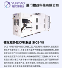
Xiamen Yunmao's large-scale silicon carbide epitaxial equipment technology breaks through!​


The SICE-Y8 Silicon Carbide Epitaxial CVD System is designed for 8-inch SiC epitaxial growth and is capable of P&N doping. The reaction chamber utilizes a horizontal hot-wall design with a proprietary inlet nozzle design and rotation mechanism, providing a stable reaction gas flow field. Induction coil heating, combined with proprietary heating graphite elements, maintains a uniform temperature field within the reaction chamber, ensuring excellent process performance. The SICE-Y8 is capable of epitaxial growth of 6/8-inch silicon carbide, a third-generation semiconductor material. It is used in the manufacture of wide-bandgap power devices, power electronics applications such as new energy vehicles, DC charging stations, photovoltaic power generation, and wind power generation, as well as rail transportation applications such as traction converter systems.

1754091308240.png

Please, Log in or Register to view URLs content!
 

tokenanalyst

Brigadier
Registered Member

HuaDa Empyrean Launches Empyrean Storm®, an Advanced Packaging Layout Design Solution​


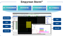
According to the official WeChat account of HuaDa Empyrean, to address the pain points of advanced packaging design routing, slow traditional layout tools, inefficient DFM requirements processing, and cumbersome physical verification processes, HuaDa Empyrean has announced the launch of Empyrean Storm®, an advanced packaging layout design solution. As a revolutionary EDA tool, it can directly address the core issues of traditional packaging design, significantly improve design efficiency, and push advanced packaging design into a new stage!

Empyrean Storm® is a layout platform designed specifically for advanced packaging design, featuring automated routing and physical verification. It supports cross-process packaging layout data import and design editing, and is deeply compatible with mainstream Silicon Interposer and Organic RDL processes. It enables large-scale automated routing of multiple chips for communication protocols like HBM and UCIe. It also performs DFM layout post-processing, such as dummy filling, to ensure mass production. It also features seamlessly integrated cross-process physical verification, Argus, ensuring layout accuracy through DRC/LVS checks.

1754091816972.png


With the above powerful functions, Storm can easily handle large-scale, high-density interconnection routing and complex layout requirements between multiple chips, inject strong power into advanced packaging design with efficient platform performance, and help design work achieve a qualitative leap.

HuaDa JiuTian's layout design solution, the Empyrean Storm platform, offers significant advantages in advanced packaging design. For example, traditional tools can take up to two to three months, or 60-90 days, to process high-speed interfaces such as HBM2/2E/3 and UCl. Storm's auto-routing engine can complete micro-bump and TSV cross-layer routing for up to 200,000 I/Os in just 15 days. The platform efficiently handles TSV routing, micro-bump connections, and BGA placement, while supporting physical verification of interposers and substrates and being compatible with CoWoS (Chip on Wafer on Substrate) architectures. One customer case study demonstrated that after configuring the tool's parameter options, the auto-routing function can complete a design iteration in just 10 minutes, significantly improving the efficiency of repeated revisions. "Storm effectively resolves design bottlenecks for advanced packaging, increasing efficiency by 1-2 months."

1754091727991.png
1754091786565.png

Please, Log in or Register to view URLs content!
 

ansy1968

Brigadier
Registered Member
Competition is Good ;)

There is a FEL project in Dalian
SSMB in Beijing

Looks like the FEL project is ahead with this recent breakthrough.


Please, Log in or Register to view URLs content!

Please, Log in or Register to view URLs content!

Please, Log in or Register to view URLs content!

Please, Log in or Register to view URLs content!


12 hours ago — Chinese scientists stably operated an electron beam at a repetition rate of one megahertz for the first time on July 24 in Dalian, ...


Dalian Coherent Light Source​

Please, Log in or Register to view URLs content!


“Comprehensive experimental research equipment base on tunable EUV coherent light source (Dalian Coherent Light Source, DCLS)” is supported by National Natural Science Foundation of China and developed jointly by Dalian Institute of Chemical Physics and Shanghai Institute of Applied Physics, CAS. the project is in the charge of Academician Xueming Yang.
DCLS is the first Free Electron Laser (FEL) user facility in China, and also the only FEL facility operating exclusively in the EUV wavelength region all over the world. Free electron laser, which is called the Fourth-generation Advanced Light Source, has become more and more important in the scientific research. It is a kind of large-scale scientific facility that hold great promise for the generation of coherent short-wavelength radiation with ultra-high brightness and ultra-short pulse duration, could dramatically improve the temporal and spatial resolution of the scientific research. With the outstanding properties, scientists could probe the microscopic world at the atomic and molecular level and on a femtosecond time scale, such as the electronic dynamic motion, molecular structure and evolution, and material phase transition. The extreme ultraviolet (EUV) wavelength region is an ideal light source for excitation of valence electrons and ionization of molecular systems with high efficiency. Such EUV light source will be a great tool for studies of important dynamic progresses in the areas of energy, chemistry, physics, material, etc.
During the past several years, the joint project team has completed a lot of important technique breakthroughs and successfully built the light source facility. It had emitted the first EUV light beam based on the sincerely cooperation between the two research teams. The gain curve and spectrum of self-amplified spontaneous emission (SASE) and high gain harmonic generation (HGHG) FEL were both measured, and tapering undulator helps increase the power by almost 100% when the FEL output saturated. It is able to deliver optical beam from 50-150nm in picoseconds or 100 femtoseconds for such research. Single pulse could contain more than 1014 photons.
In the future, DCLS could be expected to be the edge tool to promote the development of science and technology in China. In addition, 90% of the instruments and equipments in the light source are independently developed, which represents that China has reached the international advanced level in this field, and has the ability to lead the global FEL’s development.
 
Top