You are using an out of date browser. It may not display this or other websites correctly.
You should upgrade or use an alternative browser.
You should upgrade or use an alternative browser.
Chinese semiconductor thread II
- Thread starter vincent
- Start date
Only 1/4th the speed of the fastest Broadcom/NVIDIA switches though
H3C, a subsidiary of Unigroup, released the 800G National Core Intelligent Computing Switch H3C S9825-8C-G. It is equipped with domestically produced 25.6T high speed network chip, with localization rate of over 95%
cross posting with EV thread, but Chinese SiC suppliers not only crushed Wolfspeed, but also Renesas. Pushed it out of SiC and several EV related chip area.
The launch meeting of the key special project of the National Key R&D Program "Strategic Science and Technology Innovation Cooperation" was successfully held
The launch meeting and implementation plan demonstration meeting of the key project of the National Key R&D Program "Strategic Science and Technology Innovation Cooperation" - "EUV Interference Lithography Technology Research Based on High-Power High-Order Harmonics" was held at ShanghaiTech University. Members of the project expert group, project backbones, representatives of supporting units and foreign cooperation units attended the meeting.
The project " Research on Extreme Ultraviolet Interference Lithography Technology Based on High-Power High-Order Harmonics" is supported by ShanghaiTech University, the domestic partner is the Shanghai Institute of Optics and Precision Mechanics of the Chinese Academy of Sciences, and the international partner is the Paul Scherrer Institute of Switzerland. The project will be implemented from January 2025 to December 2027. The project focuses on the testing difficulties of extreme ultraviolet photoresist sensitivity and patterning capabilities, and develops high-power extreme ultraviolet light sources and high numerical aperture interference lithography devices based on high-order harmonic technology to provide a desktop exposure platform for photoresist performance testing.
The project " Research on Extreme Ultraviolet Interference Lithography Technology Based on High-Power High-Order Harmonics" is supported by ShanghaiTech University, the domestic partner is the Shanghai Institute of Optics and Precision Mechanics of the Chinese Academy of Sciences, and the international partner is the Paul Scherrer Institute of Switzerland. The project will be implemented from January 2025 to December 2027. The project focuses on the testing difficulties of extreme ultraviolet photoresist sensitivity and patterning capabilities, and develops high-power extreme ultraviolet light sources and high numerical aperture interference lithography devices based on high-order harmonic technology to provide a desktop exposure platform for photoresist performance testing.
Qingdao Rui Intelligent Semiconductor Advanced Equipment R&D and Manufacturing Center went into production
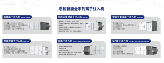
The Qingdao Sirui Intelligent Semiconductor Advanced Equipment R&D and Manufacturing Center was completed and put into production in Qingdao Free Trade Zone. As a major project of Shandong Province and a key project of Qingdao City for two consecutive years in 2024 and 2025, the Sirui Intelligent Semiconductor Advanced Equipment R&D and Manufacturing Center was jointly built by Sirui Intelligent and Qingdao Urban Investment Group. The project covers a total area of about 95 acres, with a total construction area of 86,000 square meters. The planned investment exceeds 1.2 billion yuan, focusing on the research and development and mass production of two core semiconductor front-end equipment: atomic layer deposition (ALD) and ion implantation machine (IMP). The commissioning of the center fills the gap in Qingdao's core semiconductor equipment field, marking an important step for Qingdao in the field of independent innovation and high-end equipment manufacturing in the semiconductor industry.
Sirui Intelligent Semiconductor Advanced Equipment R&D and Manufacturing Center is not only a production base with an annual output of 100 equipment, but also a key node in building a closed loop of "technology-manufacturing-ecology". The company will rely on the center to accelerate the breakthrough of key technical bottlenecks such as ALD and IMP, and deepen its layout in the fields of integrated circuits and power compounds. At the same time, Sirui Intelligent will continue to increase R&D investment, deepen cooperation with governments, universities and overseas institutions, build a world-leading R&D verification platform and talent gathering area, and help China's semiconductor industry chain to be independent and controllable.
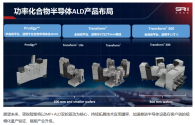
SIRUI completed the acquisition of 100% equity of Beneq, the birthplace of ALD technology. SIRUI and its subsidiary BENEQ have nearly 480 patents worldwide, and have strong technical accumulation in ALD and IMP technology and applications. They are one of the few mid-to-high-end semiconductor equipment manufacturers in China with the ability to expand global customers. Their business scope covers 40 countries and regions around the world, with a total of more than 500 global customers.
Sirui Intelligent Semiconductor Advanced Equipment R&D and Manufacturing Center is not only a production base with an annual output of 100 equipment, but also a key node in building a closed loop of "technology-manufacturing-ecology". The company will rely on the center to accelerate the breakthrough of key technical bottlenecks such as ALD and IMP, and deepen its layout in the fields of integrated circuits and power compounds. At the same time, Sirui Intelligent will continue to increase R&D investment, deepen cooperation with governments, universities and overseas institutions, build a world-leading R&D verification platform and talent gathering area, and help China's semiconductor industry chain to be independent and controllable.

SIRUI completed the acquisition of 100% equity of Beneq, the birthplace of ALD technology. SIRUI and its subsidiary BENEQ have nearly 480 patents worldwide, and have strong technical accumulation in ALD and IMP technology and applications. They are one of the few mid-to-high-end semiconductor equipment manufacturers in China with the ability to expand global customers. Their business scope covers 40 countries and regions around the world, with a total of more than 500 global customers.
A-chip's first TArray equipment shipped to advanced packaging customers
A-Semi Semiconductor shipped its first mass testing equipment to an advanced packaging customer in East China. This product delivery marks the further expansion of A-Semi's technology and product layout from the front-end wafer measurement field to the advanced packaging mass testing field. With its leading innovation capabilities, A-Semi continues to empower key areas of the semiconductor industry. In the wave of the accelerated rise of domestic semiconductor equipment, it provides new support for improving the domestic high-end mass testing equipment system and enhancing the independent controllable capabilities of each link in the industrial chain.
With the rapid development of artificial intelligence (AI), high-performance computing (HPC) and large models, the demand for data processing speed and bandwidth has exploded. As a revolutionary 3D stacked storage technology, high-bandwidth memory (HBM) has broken through the bandwidth and capacity bottlenecks of traditional memory and has become a key component supporting computing cores such as GPUs and AI accelerator cards. Its outstanding performance makes it play an indispensable role in cutting-edge fields such as training large models, running complex AI reasoning and scientific computing. However, HBM's complex multi-layer stacking structure and sophisticated interconnection process also put forward unprecedented stringent requirements on precision control and yield assurance in the manufacturing process.
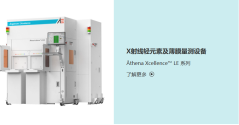
The product shipped this time, the Åthena Xcellence® TArray series (hereinafter referred to as ÅX-TArray), is a multifunctional X-ray fluorescence spectroscopy (XRF) measurement equipment designed for advanced packaging. With its innovative multi-channel multi-detector architecture and high-precision, high-speed XRF analysis capabilities, it can accurately measure the metal components of micro-bumps, multi-layer film thickness and composition, and provide non-destructive measurement data for key core process links such as planarization (CMP) uniformity control and copper interconnect structure integrity verification in HBM manufacturing. Enabling customers to achieve efficient and accurate measurement and process control of complex packaging structures is a solution to ensure high yield and high reliability of HBM products.

Driven investment of about 4.5 billion Starcom Semiconductor "Chip Test and Packaging Base Project" signed in Foshan
According to news released by Chancheng, on June 27, Foshan Starcom Semiconductor Co., Ltd. won the auction for an industrial plot of about 90 acres located in the Nanzhuang High-end Precision Intelligent Manufacturing Industrial Park in Chancheng District. The project is expected to drive an investment of about 4.5 billion yuan, and the annual output value after reaching full production will reach 3 billion yuan. It will create the largest chip testing and packaging base in the Greater Bay Area.
It is reported that the first phase of the project plans to deploy high-performance Wire Bond computing, logic, and storage chips (such as BGA/QFN/LQFP and other packaging forms), as well as advanced packaging based on flip chip technology (such as FCCSP/SiP/FCBGA, etc.); the second phase of the project will further expand to the industry's cutting-edge technologies, including bumping, through silicon via (TSV), chiplet, and 2.5D/3D packaging technology. After the project is completed, the process level will rank first in the country.
Foshan Xingtong Semiconductor Co., Ltd. is a company that specializes in the manufacture, sales and technology development of integrated circuit chips, semiconductor products and electronic components. It plans to build an integrated circuit chip semiconductor manufacturing base, including production bases, test packaging bases, and R&D centers for integrated circuit chips, semiconductor products and electronic components.
Pinghu Laboratory: 8-inch SiC project reaches a critical node.
8-inch SiC platform tape-out successful
On June 27, Shenzhen Pinghu Laboratory revealed on its official Weibo that they had joined hands with Shenzhen Pengjin High-tech Co., Ltd. to successfully overcome the core technical difficulties of 1200V trench gate SiC MOSFET chips, built an 8-inch process platform, and achieved the successful tape-out of high-performance 1200V trench gate SiC MOSFET chips with independent intellectual property rights .
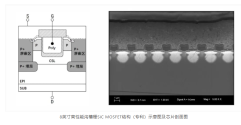
8- inch high-performance trench gate SiC MOSFET structure (patent) schematic diagram and chip cross-section
It is understood that the core invention patent (patent publication number : CN118610269A) has been authorized, and its breakthrough results have many highlights:
- The static performance indicators achieve the industry-leading low specific on-resistance (<2.1mΩ·cm²), which is better than the technical level of mainstream international high-reliability manufacturers (such as Bosch G2).
- The chip has a reverse breakdown voltage greater than 1500V , a threshold voltage that is stable at 3.3V, and has achieved commercially valuable yield demonstration on an 8-inch wafer .
- We have successfully overcome many SiC trench process challenges on 8-inch wafers , including MeV-level high-energy ion implantation, fixed-orientation etching, gate oxide region thickness distribution modulation , low-defect high-temperature annealing, low- resistance ohmic contact , and high-reliability passivation , achieving mass production-level process control .
- We have successfully built a full-process, independently controllable 8-inch trench gate SiC MOSFET process platform that is domestically leading and internationally advanced. The CP yield of 1200V 40mΩ -level trench gate SiC MOSFET wafersis over 90%, with the highest single-chip yield reaching 96%.
- The simulation and manufacturing alignment of the process platform has been basically completed. From the core cell structure to the terminal protection structure , the full set of dynamic and static simulations are consistent with the measured data by more than 95%.
It is understood that the Shenzhen Pinghu Laboratory has built the country's first open and shared power semiconductor platform that integrates 8-inch SiC/GaN scientific research and pilot production, covering the entire chain of third-generation power semiconductor substrates, epitaxy, device preparation, packaging testing, failure analysis, and reliability verification. It has built an advanced 8-inch process platform with backward compatibility.
The localization of Chinese semiconductor materials accelerates, putting pressure on Taiwanese manufacturers
According to legal reports, the annual production capacity of 8-inch and 12-inch silicon wafers in mainland China will grow from 22 million pieces in 2024 to 24 million and 38 million pieces in 2027, respectively.
The agency estimates that by 2027, the local 12-inch wafer supply coverage in mainland China will increase from 41% to 54%, and the 8-inch will increase from 64% to 78%.
Although Japan's Shin-Etsu Chemical is still the main supplier of high-end 12-inch wafers, and the company's revenue share in mainland China has remained at 8% to 11% since 2019, local manufacturers in mainland China are catching up rapidly and their market share is significantly expanding.
Indeed until one year ago SMIC top 7nm wafers (and photoresist) were still from Japan, maybe also today they still buy top quality 12" wafers from Japan...
Nobody knows for how long this faucet will remain open for SMIC, hopefully they are not far from localizing the whole wafer supply chain and chemicals....
