Chinese semiconductor thread II

tokenanalyst

Brigadier
Registered Member
Can China pirate the EDA software and continue to use it? Softwares are easy to pirate.

Depends on the software, TCAD, circuits simulators and layout tools are easier to pirate, but there is a lot of tools that require constant servicing from the EDA vendor and a lot of IP like PDKs, EDA companies make more money selling services than selling tools. Lithography optimization software tools like require collaboration between the EDA provider, the FAB and the mask producer.

So at the end a lot can be pirated but if you are big design house the last thing you want is legal trouble. EDA piracy was a big deal back in the old days like in 2000s and 2010s, like almost half of EDA tools used being pirated especially in Asia. Western and Japanese make a big deal out of it.

What I think is going to happen like semiconductor equipment tools, companies like SMIC, HLMC and local IC houses are going to collaborate more with local providers like Empyrean EDA and Oriental Jingyuan Microelectronics to streamline their tooling to a local workflow and create localized IP and PDKs. Once that happen is game over for US companies, reconquer their past dominance in the Chinese market will be an uphill battle once every Chinese design house move their IP to localized EDA workflows and IPs. And even worse once Chinese companies focus their efforts to conquer IC design markets outside of China.
 
Last edited:

tokenanalyst

Brigadier
Registered Member

Guangzhou Tonoshi Technology's gallium oxide epitaxial project is about to start production.​


According to the Hong Kong University of Science and Technology Express, recently, "Tonoshi Technology", jointly incubated by the Hong Kong University of Science and Technology Fok Ying Tung Institute and the Hong Kong University of Science and Technology (Guangzhou), ushered in a milestone moment - its first advanced production plant in Nansha was officially put into use! The plant is equipped with high-standard clean room facilities and complete production and R&D supporting facilities, with batch epitaxial preparation capabilities, realizing "from laboratory to industry", and laying a solid foundation for the large-scale promotion of gallium oxide epitaxial products to the market.

The production plant of Tonoshi Technology is located in Nansha, Guangzhou, the "golden inner bay" of the Guangdong-Hong Kong-Macao Greater Bay Area, covering an area of about 500 square meters, integrating R&D, testing, manufacturing, and process support. It is equipped with an MOCVD process area and ion implantation room, a dedicated gas storage room, and a solid waste treatment room to fully ensure the stability and safety of high-tech product manufacturing.

Please, Log in or Register to view URLs content!
 

tokenanalyst

Brigadier
Registered Member

AMEC successfully held the 2024 and 2025 first quarter performance briefing​


AMEC has developed one successful etching equipment and thin film equipment after another, quickly entered the market, and provided highly competitive and cost-effective equipment products for customers of integrated circuits and pan-semiconductor micro devices, and continuously increased market share. The company has accumulated more than 6,000 plasma and chemical film reaction tables, and has achieved mass production and large-scale repetitive sales on 137 production lines at home and abroad.

According to market and customer needs, the company has significantly increased its R&D efforts. Currently, the company's research and development projects cover six categories and the development of more than 20 new equipment. The company's speed of developing new products has significantly accelerated. In the past, it usually took three to five years to develop a new equipment. Now it only takes two years or less to develop competitive new equipment and successfully enter the market. In 2024, the company's total R&D investment reached 2.45 billion yuan, an increase of 94.3% over 2023, accounting for about 27% of operating income, which is much higher than the average R&D investment of 10% to 15% of revenue of companies listed on the Science and Technology Innovation Board.

In 2024, the company achieved operating income of approximately 9.065 billion yuan, an increase of approximately 2.802 billion yuan from 2023. On the basis of maintaining an average annual growth rate of operating income of more than 35% in the past 13 years and an average annual growth rate of operating income of more than 40% in the past four years, the company's operating income in 2024 increased by approximately 44.73% year-on-year. Among them, the revenue of etching equipment was approximately 7.277 billion yuan. On the basis of an average annual growth rate of more than 50% in the past four years, it increased by approximately 54.72% year-on-year in 2024. The company's comprehensive competitive advantages continued to be strengthened and improved, and the KPI indicators of various operations have been comparable to the international advanced level, and even exceeded the level of international leading semiconductor equipment companies in key indicators such as on-time delivery and defects per unit. AMEC focused on improving labor productivity. On the basis of achieving per capita sales of 3.5 million yuan in 2022, per capita sales exceeded 4 million yuan in 2024, reaching the international advanced level of the equipment industry.

Dr. Yin Zhiyao shared that AMEC is currently developing a more competitive new generation of high-energy CCP plasma etching equipment, a new generation of ICP low-energy plasma etching equipment, wafer edge etching equipment, a new generation of plasma source PECVD equipment, LPCVD and ALD thin film equipment, epitaxial EPI equipment and electron beam quantity detection equipment for integrated circuit micro-manufacturing. In recent years, with the rapid development of the advanced packaging market, AMEC's product layout for advanced packaging has also shifted from CCP plasma etching equipment and TSV deep silicon etching equipment that have entered the production line in batches to the development of PVD, CVD and quantity detection equipment, etc., to provide customers with comprehensive solutions. AMEC has also been continuously deploying the pan-semiconductor micro-manufacturing field for more than a decade, including the manufacture of gallium nitride-based light-emitting diodes, MOCVD equipment for Mini-LED and Micro-LED, and MOCVD equipment for the manufacture of silicon carbide and gallium nitride power devices. AMEC decided to develop large flat-panel equipment at the end of 2023 to fill the gap in this field in China as soon as possible. These include core thin film and plasma etching equipment required in the field of new display technology, and have made much progress ahead of schedule.

The new 180,000 square meter R&D and production base built by AMEC in Shanghai Lingang New Area will achieve an annual output value of RMB 8.5 billion in 2024, the first year of mass production. The 140,000 square meter production and R&D base built by Nanchang AMEC in the High-tech Zone will reach an annual output value of RMB 6.1 billion in 2024. AMEC's 100,000 square meter headquarters twin tower building will be completed in Dishui Lake, Lingang by the end of this year. With the rapid expansion of product lines, in order to get closer to customers, AMEC plans to build production and R&D bases in Zengcheng District, Guangzhou and Chengdu High-tech Zone to ensure that there are enough factories in the next ten years to meet the needs of many new product development and rapid growth in production capacity.

Please, Log in or Register to view URLs content!
 

JPaladin32

New Member
Registered Member
I'm usually not a pessimist but I personally don't think we should read too much into '5nm'. Whatever the packaging is, X90 is very likely just another N+2 chip. The '5nm' claim was probably just a mistake from the news editor of state media. State media is still media and they do make mistakes sometimes, my reasons being:

1. X90 has a much larger die (shown in Geekerwan's recent post) and it doesn't make sense to start on a new process on large dies. Normally it's done on smaller ones first for better yields.
2. X90 is a Kirin 9010 based design which came out early last year. Back then 5nm was not ready. The laptop itself was rumored to be released late last year but was delayed due to software ecosystem maturity. The chip was probably fabbed last year, not recently.
3. X90 has almost the exact CPU frequencies as the 7nm Kirin 9010. Process node improvements normally bump up the CPU frequency, but on X90 there doesn't seem to be any at all.

I think 3. is the hard evidence. The moment I saw the X90 core frequencies I was pretty much convinced there won't be process changes. Packaging is a whole nother story and calling an N+2 chip '5nm' because of packaging is misleading at best. My intention is to just bring our expectations to the right level and to avoid any disappointment if we see X90 is still on N+2 process.
 

tphuang

General
Staff member
Super Moderator
VIP Professional
Registered Member
once you have the software, you can just keep using it. If you block incoming software updates, what could they possibly do to stop you from using it? Otherwise, just hack into it and remove the update codes.

Other than that, it's about time for legacy process to switch to domestic EDA tools.
 

GulfLander

Major
Registered Member
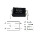
Does china has suppliers for optocoupler?
They are very basic devices, like a transistor
View attachment 153100

According to google

Shenzhen Orient Components Co., Ltd.:

A national high-tech enterprise specializing in R&D and manufacturing of optoelectronic chips and optocouplers.

Shenzhen Semilotec Co., Ltd.:

A supplier of various optocouplers, including the HCNR201-000E High Linearity Optocouplers.

Shenzhen Kento Electronic Co., Ltd.:

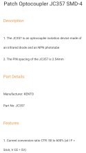
A manufacturer and supplier of the JC357 optocoupler.
 

LanceD23

Junior Member
Registered Member
According to google

Shenzhen Orient Components Co., Ltd.:

A national high-tech enterprise specializing in R&D and manufacturing of optoelectronic chips and optocouplers.

Shenzhen Semilotec Co., Ltd.:

A supplier of various optocouplers, including the HCNR201-000E High Linearity Optocouplers.

Shenzhen Kento Electronic Co., Ltd.:

A manufacturer and supplier of the JC357 optocoupler.
They are components suppliers like digikey.
They are middle men
 
Top