Chinese semiconductor thread II

interestedseal

Junior Member
Registered Member
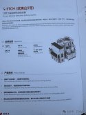
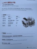
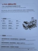
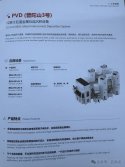
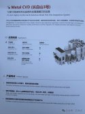
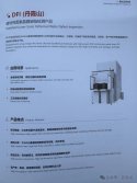
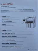
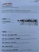
Xinkailai announced that it has completed the development of 13 types of key mass testing products and has begun mass production applications in major domestic semiconductor manufacturing companies in logic, storage and compound. Semiconductor Industry Zongheng interviewed Li Zhoujian, president of Xinkailai's mass testing equipment product line , to learn more about the core products and future layout of this low-key semiconductor equipment company.

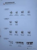
Xinkailai will release 13 categories of products covering optical detection, optical measurement, PX measurement, power detection and other fields.

The products can be divided into two categories: one is the optical measurement products with higher technical difficulty, such as bright field defect detection BFI, dark field defect detection DFI, etc. The other is PX (physical and X-ray) and power detection products that were not available in China at that time but were necessary for the production line , such as X-ray XPS, XRD, etc.

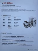
Optical measurement products, including: bright field defect detection BFI, dark field defect detection DFI, surface defect detection PC, blank mask defect detection MBI, overlay measurement DBO and IBO, have basically completed customer-side verification and will enter mass production in 2025.

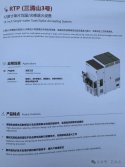
PX measurement products, including atomic force microscope measurement AFM, X-ray measurement XPS, XRD, and XRF, have all entered mass production and delivery. It is understood that Xinkailai's PX measurement products have reached the industry's advanced level in key performance indicators such as measurement accuracy, repeatability, and yield. Currently, major domestic semiconductor manufacturers of logic, storage, and compounds have all been mass-produced.

Power detection products, including CP (Chip Probing), KGD (Known Good Die) and FT (Final Test) testers, have also been developed and put into large-scale application.

Please, Log in or Register to view URLs content!

Crazy debut! Here is the product brochure. This is just the beginning. They’ll unveil more next year
 

OptimusLion

Junior Member
Registered Member
The Institute of Microelectronics of the Chinese Academy of Sciences has successfully developed a GAA transistor that is close to an ideal switch using a new stacked nanosheet channel surface treatment technology


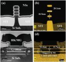
The stacked nanosheet gate-all-around (GAA) transistors have excellent gate control characteristics, higher driving performance and more circuit design flexibility. They are the core transistor structure after FinFET in mainstream integrated circuit manufacturing.

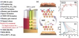
However, the current stacked nanosheet GAA devices have a large channel interface state, making it difficult to achieve ideal subthreshold switching. A key reason is that the newly introduced GeSi/Si superlattice stack is susceptible to the integrated thermal budget at the material interface, resulting in the diffusion and redistribution of Ge atoms, resulting in trace amounts of Ge atoms remaining on the surface after the nanosheet channel is released, causing additional interface defects and reduced carrier conductivity.

34ea6e65-7a41-4136-a0dc-67bc93db26de.jpg
To address this challenge, the integrated circuit pilot process research and development team of the Institute of Microelectronics, Chinese Academy of Sciences, proposed a low-temperature ozone quasi-atomic layer etch (qALE) technology that is fully compatible with the GAA transistor nanosheet channel release process.

7f7fd0c2-e0f9-4a13-b4fd-30b067da7d91 (1).jpg

It is reported that after the nanosheet channel is released, this technology can achieve precise removal of Ge atoms remaining on the surface of the nanosheet channel through extremely thin ozone self-limiting oxidation and corrosion reaction, thereby avoiding damage to the inner Si channel.

da45203a-db04-49ae-980a-59ea0ceecc84.jpg
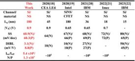
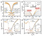
The characteristics of the CMOS device developed by the Institute of Microelectronics of the Chinese Academy of Sciences show that after low-temperature qALE treatment, the interface state density of the nanosheet channel is reduced by two orders of magnitude, the subthreshold switching swing of the transistor is optimized to 60.3 mV/dec, almost close to the theoretical thermodynamic limit of the device (60mV/dec), and the leakage current (Ioff ) is reduced by 66.7%.

At the same time, since the carrier scattering caused by the surface charge of the channel is significantly reduced after treatment, the transistor on-state current (I on ) is also increased by more than 20%. This research work provides an efficient and low-cost technical path for the preparation of high-performance stacked nanosheet GAA devices.

17aff5b1-00b0-49b0-b6a9-56e813384c50.jpg

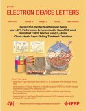
The relevant research results have been published in the latest IEEE Electron Device Letters in March and were successfully selected as the cover paper of the journal

IMG_20250326_124322_195.jpg

Graduate students Jiang Renjie and Sang Guanqiao from the Institute of Microelectronics are the first authors of the paper, and researchers Zhang Qingzhu and Yin Huaxiang are co-corresponding authors. This research was supported by the Strategic Priority Research Program (Class A) of the Chinese Academy of Sciences and the National Natural Science Foundation of China.

Please, Log in or Register to view URLs content!
 

OptimusLion

Junior Member
Registered Member
Dongfang Jingyuan DR-SEM r655: Technological innovation drives the upgrade of domestic testing equipment

Oriental Jingyuan has been deeply engaged in the field of electron beam inspection for many years. Its electron beam defect inspection equipment EBI and key dimension measurement equipment CD-SEM have successively achieved zero breakthroughs in domestic substitution and won market recognition.

At the beginning of 2023, Oriental Jingyuan launched DR-SEM r600, equipped with 3-channel electronic imaging technology and a new equipment platform, and completed mass production verification on the client side, laying the foundation for subsequent development. After two years of iterative research and development, Oriental Jingyuan's latest generation of DR-SEM r655 products will be equipped with a new high-performance electron gun and optical detection module, as well as an upgraded film transmission system and algorithm system, breaking through a series of technical difficulties and meeting the application needs of domestic advanced process production lines.

032d80722598b244c21d48dcc486740c.jpg

Please, Log in or Register to view URLs content!
 
Top