You are using an out of date browser. It may not display this or other websites correctly.
You should upgrade or use an alternative browser.
You should upgrade or use an alternative browser.
Chinese semiconductor thread II
- Thread starter vincent
- Start date
China Micro's (AMEC) revenue in the first half of the year was 4.961 billion yuan, a year-on-year increase of 43.88%.
On the evening of August 28, China's leading semiconductor equipment manufacturer, AMEC (688012), released its 2025 semi-annual report.
The financial report shows that in the first half of the year, China Micro Corporation achieved operating income of approximately 4.961 billion yuan, an increase of approximately 43.88% year-on-year; net profit attributable to shareholders of the parent was 706 million yuan, an increase of 36.62% year-on-year; and net profit excluding non-recurring items was 539 million yuan, an increase of 11.49% year-on-year.
R&D investment in the first half of the year was 1.492 billion yuan
In terms of R&D investment, the announcement showed that in the first half of this year, China Micro Corporation's R&D investment totaled 1.492 billion yuan, an increase of 53.70% over the same period last year. The total R&D investment accounted for 30.07% of operating income, an increase of 1.92 percentage points over the same period last year.
Market performance and shipment volume of various equipment
AMEC is primarily engaged in the research, development, production, and sales of high-end semiconductor and pan-semiconductor equipment. Its plasma etching equipment is already used in 65- to 5-nanometer (nm) and other advanced integrated circuit manufacturing and packaging lines for international first-tier clients. To meet the more stringent process requirements of 5nm and below, the company is actively developing next-generation models to achieve higher etch selectivity and uniformity control, as well as more stable mass production performance. In memory chip manufacturing, AMEC's plasma etching equipment is already widely used in the mass production of advanced 3D flash memory and dynamic random access memory devices.
1. CCP etching equipment
The company's CCP etching equipment, including dual-reactor models Primo D-RIE, Primo AD-RIE, Primo AD-RIE-e and single-reactor model Primo HD-RIE, has been widely used in the production lines of domestic and foreign first-line customers. The single-reactor product Primo HD-RIE-e for high-precision and high-selectivity etching processes and Primo UD-RIE for ultra-high aspect ratio etching processes continue to receive customer orders. Among them, Primo HD-RIE-e has been installed in more than 120 reaction tables in the first half of 2025, and Primo UD-RIE has been installed in nearly 200 reaction tables.
As of the first half of 2025, the cumulative installed base of CCP etching equipment exceeded 4,500 reactors, an increase of over 900 reactors compared to the same period in 2024. Dual-reactor etching products, with their unique design, provide balanced solutions for customers at both mature and advanced technology nodes, consistently securing volume orders. As of the first half of 2025, the cumulative installed base exceeded 3,300 reactors. Single-reactor products have achieved continuous breakthroughs in key processes in recent years, reaching a cumulative installed base of nearly 1,200 reactors as of the first half of 2025.
2. ICP etching equipment
During the reporting period, the company's ICP etching equipment entered mass production on the production lines of more than 50 customers, covering chips and devices such as logic, DRAM, 3D NAND, power and power management, and micro-electromechanical systems. The company also continued to validate additional ICP etching processes. As of the first half of 2025, the cumulative installed base of ICP etching equipment exceeded 1,200 reactors.
3. MOCVD equipment
During the reporting period, the company's products, such as PRISMO A7 for blue light lighting, PRISMO HiT3 for deep ultraviolet LEDs, and PRISMO UniMax for Mini-LED displays, continued to serve customers, and the company continued to maintain its leading position in the international GaN-based MOCVD equipment market.
Production capacity continues to expand
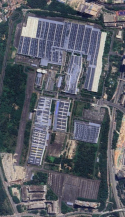
The company's approximately 140,000 square meter production and R&D base in Nanchang and approximately 180,000 square meter production and R&D base in Shanghai Lingang have been put into use, significantly increasing production capacity; the approximately 100,000 square meter headquarters building and R&D center on the shores of Dishui Lake in Shanghai Lingang is also under smooth construction; to ensure sufficient factory space in the next ten years and to meet the needs of numerous new product developments and rapid production capacity growth, the company plans to build new production and R&D bases in Zengcheng District, Guangzhou and Chengdu Hi-tech Zone.
More than 20 new equipment are under development to build a platform-based group company
In terms of new product research and development, AMEC’s current projects cover six types of equipment and involve the development of over 20 new devices.
AMEC aligns closely with market trends and is expanding the application scope of its MOCVD equipment. Development of MOCVD systems for red and yellow LEDs is progressing smoothly, with laboratory tests showing excellent wavelength uniformity. During the reporting period, AMEC shipped its first such system to a leading domestic customer for production validation.
The next-generation MOCVD equipment for GaN-on-silicon power devices is on track. Compatible with both 6-inch and 8-inch processes, it offers improved thickness and composition uniformity, superior epitaxial wafer surface particle control, and automated handling. Equipment for SiC power device epitaxy is also in development.
AMEC has commercialized six thin-film deposition products. Its tungsten tool suite—comprising CVD, HAR, and ALD tungsten tools—covers all tungsten applications in memory devices. These systems have passed field verification at key memory clients, meeting performance needs for advanced metal interconnects (including high aspect ratio) and wordlines in 3D memory, securing repeat orders. The products also meet requirements for tungsten contact applications in advanced logic devices, with shipments to multiple logic customers and ongoing successful verification.
A series of metal gate solutions—ALD titanium nitride, ALD titanium aluminum, and ALD tantalum nitride—are now available for advanced logic devices. These have completed device validation across multiple advanced logic customers, achieving world-leading film uniformity, contamination control, and production efficiency. Equipment has been shipped to customers and is progressing smoothly toward approvals.
Building on existing R&D in metal CVD and ALD equipment, AMEC is advancing multiple new CVD and ALD systems to broaden thin-film equipment coverage and market share.
Through fundamental research and customer-driven technical feedback, AMEC’s EPI R&D team has developed a proprietary platform featuring innovative pretreatment and epitaxial reaction chambers. Low-pressure EPI equipment has been shipped to mature process customers for mass production verification and is now entering advanced process validation. The new high-selectivity pre-cleaning chamber meets advanced process demands and has been delivered to advanced process customers, progressing through customer verification. Atmospheric pressure EPI equipment has completed development and entered process debugging; atmospheric pressure EPI systems have completed development and entered process verification.
Yin Zhiyao, Chairman of AMEC, said: "Our new equipment development speed has significantly accelerated—what once took three to five years now takes two years or less, enabling rapid market entry and mass production. Currently, over 30 types of equipment cover 25% to 30% of high-end semiconductor equipment. Over the next five to ten years, through organic growth and external expansion, we aim to capture 50% to 60% of the high-end semiconductor equipment market, becoming a platform-based group company."
The Institute of Microelectronics of the Chinese Academy of Sciences has successfully developed a complementary single-crystal silicon vertical channel transistor (CVFET).
According to the International Roadmap for Devices and Systems (IRDS2023), the complementary field-effect transistor (CFET) is the next-generation transistor architecture in integrated circuit logic technology, following FinFET and horizontal GAA . CFET technology vertically stacks NMOS and PMOS devices, changing the traditional planar process or horizontal FinFET/GAA layout to achieve higher integration density and better performance in a smaller space.
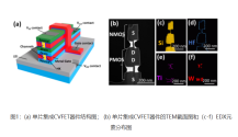
The Institute of Microelectronics recently proposed and developed a monolithically integrated complementary vertical channel transistor (CVFET) structure based on independently developed vertical channel technology. This structure utilizes a double-flank technique compatible with CMOS fabrication processes. Through a two-step epitaxial growth process, the nanosheet channel thickness and gate length are controlled independently, enabling the self-aligned integration of n-type and p-type nanosheet transistors stacked on top of each other. The electrical characteristics of the structure are as follows: the subthreshold swing (SS) of the upper and lower (NMOS/PMOS) devices is 69 mV/dec and 72 mV/dec, respectively; the drain-induced barrier lowering (DIBL) is 12 mV/V and 18 mV/V, respectively; and the current on/off ratio (Ion/Ioff) is 3.1×10⁶ and 5.4× 10⁶ , respectively . Its CMOS inverter can achieve normal signal phase inversion function. At a power supply voltage (VDD) of 1.2 V, the inverter gain is 13 V/V; at an operating voltage of 0.8 V, the high-level noise margin (NMH) and low-level noise margin (NML) are 0.343 V and 0.245 V, respectively.
The Institute of Microelectronics has made important progress in the research direction of chip integrated electromigration EDA tools
With the rapid development of high-performance artificial intelligence algorithms, chiplet integration systems have become a highly promising technology solution due to their ability to meet the demands of massive data transmission. This technology offers significant advantages, including high-speed interconnection and bandwidth, reduced cross-package interconnection, and low cost and high performance, making it widely popular. However, chiplet integration is plagued by issues such as high power supply current and heat dissipation, resulting in severe electromigration reliability challenges. For chiplet integration systems with highly complex process layers, achieving accurate and efficient electromigration simulation and coupled analysis of electromigration and thermal effects has become a key research area in the field of advanced packaging reliability EDA tools.
To address these challenges, a collaborative team from the EDA Center of the Institute of Microelectronics, Chinese Academy of Sciences, developed a coupled electromigration-thermal simulation model for TSV interconnects in chip-to-chip integrated systems. This model utilizes the finite-difference time-domain (FDTD) method to establish a comprehensive electro-thermal-stress analysis approach covering the entire electromigration void nucleation and growth process, enabling accurate calculation of the hydrostatic stress induced by electron flow. The study also constructed a full-chip thermal model of the heterogeneous integrated system, including a heat sink, and applied the finite volume element method (FVM) for global electro-thermal co-simulation. This significantly improved computational efficiency while strictly adhering to the conservation principles of the heat conduction equation. Crucially, by integrating electromigration-thermomigration simulations with Joule heating, the model can analyze the interplay between stress evolution, void growth, resistance change, and Joule heating within a unified framework. Model validation results demonstrate a simulation error of only 0.61% compared to the commercial finite element tool COMSOL. Compared to experimental data, the model significantly reduces the electromigration lifetime prediction error by 76.4% compared to existing mainstream methods. The model can also accurately reflect the dominant role of temperature and current density on the electromigration process at different analysis stages.
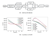
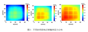
This research, titled "ChipletEM: Physics-Based 2.5D and 3D Chiplet Heterogeneous Integration Electromigration Signoff Tool Using Coupled Stress and Thermal Simulation," was presented orally at the 62nd International Design Automation Conference (DAC). Researcher Sun Zeyu is the first author of the paper, and Researcher Xu Qinzhi and Researcher Li Zhiqiang of the EDA Center of the Institute of Microelectronics are co-corresponding authors. This research was funded by the Strategic Priority Research Program (A) of the Chinese Academy of Sciences, the National Natural Science Foundation of China, and the Young Interdisciplinary Research Team of the Chinese Academy of Sciences.
To address these challenges, a collaborative team from the EDA Center of the Institute of Microelectronics, Chinese Academy of Sciences, developed a coupled electromigration-thermal simulation model for TSV interconnects in chip-to-chip integrated systems. This model utilizes the finite-difference time-domain (FDTD) method to establish a comprehensive electro-thermal-stress analysis approach covering the entire electromigration void nucleation and growth process, enabling accurate calculation of the hydrostatic stress induced by electron flow. The study also constructed a full-chip thermal model of the heterogeneous integrated system, including a heat sink, and applied the finite volume element method (FVM) for global electro-thermal co-simulation. This significantly improved computational efficiency while strictly adhering to the conservation principles of the heat conduction equation. Crucially, by integrating electromigration-thermomigration simulations with Joule heating, the model can analyze the interplay between stress evolution, void growth, resistance change, and Joule heating within a unified framework. Model validation results demonstrate a simulation error of only 0.61% compared to the commercial finite element tool COMSOL. Compared to experimental data, the model significantly reduces the electromigration lifetime prediction error by 76.4% compared to existing mainstream methods. The model can also accurately reflect the dominant role of temperature and current density on the electromigration process at different analysis stages.


This research, titled "ChipletEM: Physics-Based 2.5D and 3D Chiplet Heterogeneous Integration Electromigration Signoff Tool Using Coupled Stress and Thermal Simulation," was presented orally at the 62nd International Design Automation Conference (DAC). Researcher Sun Zeyu is the first author of the paper, and Researcher Xu Qinzhi and Researcher Li Zhiqiang of the EDA Center of the Institute of Microelectronics are co-corresponding authors. This research was funded by the Strategic Priority Research Program (A) of the Chinese Academy of Sciences, the National Natural Science Foundation of China, and the Young Interdisciplinary Research Team of the Chinese Academy of Sciences.
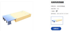
Bosu System Integration applied for a patent for a special anti-microvibration base for lithography machines, creating a broadband vibration reduction feature.
Jiangsu Bosu System Integration Co., Ltd. has applied for a patent called "A special anti-micro-vibration base for photolithography machines", publication number CN120447314A, and the application date is June 2025.
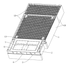
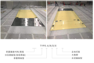
The patent abstract shows that the present invention relates to the field of photolithography machine base technology, and discloses a special anti-micro-seismic base for photolithography machines, including: two cement bases, and also including: a first cement shell, located on one side of the cement base; a first isolation module, located in the first cement shell; a lower panel, fixed above the first cement shell; a stiffening plate, fixed above the lower panel, used to play a supporting role; an upper panel, fixed on the stiffening plate; the photolithography machine anti-micro-seismic base of the present invention has a significant anti-micro-seismic effect: the upper panel and the lower panel form a symmetrical structure through the vertically distributed stiffening plates; the stiffening plate serves as the core shock-absorbing unit, and the right-angle grooves and acute-angle grooves opened thereon constitute a multi-stage vibration suppression system, and the right-angle grooves use the stress wave reflection principle to change the direction of vibration wave conduction, forcing part of the vibration energy to return to the original propagation medium; the acute-angle grooves refract and scatter the vibration waves in multiple directions based on the stress wave refraction theory, so that the vibration energy diffuses and attenuates into three-dimensional space, forming a broadband shock-absorbing characteristic.
China Micro's (AMEC) revenue in the first half of the year was 4.961 billion yuan, a year-on-year increase of 43.88%.
On the evening of August 28, China's leading semiconductor equipment manufacturer, AMEC (688012), released its 2025 semi-annual report.
The financial report shows that in the first half of the year, China Micro Corporation achieved operating income of approximately 4.961 billion yuan, an increase of approximately 43.88% year-on-year; net profit attributable to shareholders of the parent was 706 million yuan, an increase of 36.62% year-on-year; and net profit excluding non-recurring items was 539 million yuan, an increase of 11.49% year-on-year.
R&D investment in the first half of the year was 1.492 billion yuan
In terms of R&D investment, the announcement showed that in the first half of this year, China Micro Corporation's R&D investment totaled 1.492 billion yuan, an increase of 53.70% over the same period last year. The total R&D investment accounted for 30.07% of operating income, an increase of 1.92 percentage points over the same period last year.
Market performance and shipment volume of various equipment
AMEC is primarily engaged in the research, development, production, and sales of high-end semiconductor and pan-semiconductor equipment. Its plasma etching equipment is already used in 65- to 5-nanometer (nm) and other advanced integrated circuit manufacturing and packaging lines for international first-tier clients. To meet the more stringent process requirements of 5nm and below, the company is actively developing next-generation models to achieve higher etch selectivity and uniformity control, as well as more stable mass production performance. In memory chip manufacturing, AMEC's plasma etching equipment is already widely used in the mass production of advanced 3D flash memory and dynamic random access memory devices.
1. CCP etching equipment
The company's CCP etching equipment, including dual-reactor models Primo D-RIE, Primo AD-RIE, Primo AD-RIE-e and single-reactor model Primo HD-RIE, has been widely used in the production lines of domestic and foreign first-line customers. The single-reactor product Primo HD-RIE-e for high-precision and high-selectivity etching processes and Primo UD-RIE for ultra-high aspect ratio etching processes continue to receive customer orders. Among them, Primo HD-RIE-e has been installed in more than 120 reaction tables in the first half of 2025, and Primo UD-RIE has been installed in nearly 200 reaction tables.
As of the first half of 2025, the cumulative installed base of CCP etching equipment exceeded 4,500 reactors, an increase of over 900 reactors compared to the same period in 2024. Dual-reactor etching products, with their unique design, provide balanced solutions for customers at both mature and advanced technology nodes, consistently securing volume orders. As of the first half of 2025, the cumulative installed base exceeded 3,300 reactors. Single-reactor products have achieved continuous breakthroughs in key processes in recent years, reaching a cumulative installed base of nearly 1,200 reactors as of the first half of 2025.
2. ICP etching equipment
During the reporting period, the company's ICP etching equipment entered mass production on the production lines of more than 50 customers, covering chips and devices such as logic, DRAM, 3D NAND, power and power management, and micro-electromechanical systems. The company also continued to validate additional ICP etching processes. As of the first half of 2025, the cumulative installed base of ICP etching equipment exceeded 1,200 reactors.
3. MOCVD equipment
During the reporting period, the company's products, such as PRISMO A7 for blue light lighting, PRISMO HiT3 for deep ultraviolet LEDs, and PRISMO UniMax for Mini-LED displays, continued to serve customers, and the company continued to maintain its leading position in the international GaN-based MOCVD equipment market.
Production capacity continues to expand
The company's approximately 140,000 square meter production and R&D base in Nanchang and approximately 180,000 square meter production and R&D base in Shanghai Lingang have been put into use, significantly increasing production capacity; the approximately 100,000 square meter headquarters building and R&D center on the shores of Dishui Lake in Shanghai Lingang is also under smooth construction; to ensure sufficient factory space in the next ten years and to meet the needs of numerous new product developments and rapid production capacity growth, the company plans to build new production and R&D bases in Zengcheng District, Guangzhou and Chengdu Hi-tech Zone.
More than 20 new equipment are under development to build a platform-based group company
In terms of new product research and development, AMEC’s current projects cover six types of equipment and involve the development of over 20 new devices.
AMEC aligns closely with market trends and is expanding the application scope of its MOCVD equipment. Development of MOCVD systems for red and yellow LEDs is progressing smoothly, with laboratory tests showing excellent wavelength uniformity. During the reporting period, AMEC shipped its first such system to a leading domestic customer for production validation.
The next-generation MOCVD equipment for GaN-on-silicon power devices is on track. Compatible with both 6-inch and 8-inch processes, it offers improved thickness and composition uniformity, superior epitaxial wafer surface particle control, and automated handling. Equipment for SiC power device epitaxy is also in development.
AMEC has commercialized six thin-film deposition products. Its tungsten tool suite—comprising CVD, HAR, and ALD tungsten tools—covers all tungsten applications in memory devices. These systems have passed field verification at key memory clients, meeting performance needs for advanced metal interconnects (including high aspect ratio) and wordlines in 3D memory, securing repeat orders. The products also meet requirements for tungsten contact applications in advanced logic devices, with shipments to multiple logic customers and ongoing successful verification.
A series of metal gate solutions—ALD titanium nitride, ALD titanium aluminum, and ALD tantalum nitride—are now available for advanced logic devices. These have completed device validation across multiple advanced logic customers, achieving world-leading film uniformity, contamination control, and production efficiency. Equipment has been shipped to customers and is progressing smoothly toward approvals.
Building on existing R&D in metal CVD and ALD equipment, AMEC is advancing multiple new CVD and ALD systems to broaden thin-film equipment coverage and market share.
Through fundamental research and customer-driven technical feedback, AMEC’s EPI R&D team has developed a proprietary platform featuring innovative pretreatment and epitaxial reaction chambers. Low-pressure EPI equipment has been shipped to mature process customers for mass production verification and is now entering advanced process validation. The new high-selectivity pre-cleaning chamber meets advanced process demands and has been delivered to advanced process customers, progressing through customer verification. Atmospheric pressure EPI equipment has completed development and entered process debugging; atmospheric pressure EPI systems have completed development and entered process verification.
Yin Zhiyao, Chairman of AMEC, said: "Our new equipment development speed has significantly accelerated—what once took three to five years now takes two years or less, enabling rapid market entry and mass production. Currently, over 30 types of equipment cover 25% to 30% of high-end semiconductor equipment. Over the next five to ten years, through organic growth and external expansion, we aim to capture 50% to 60% of the high-end semiconductor equipment market, becoming a platform-based group company."
cool part is the 2nd part of that image. Showing that R&D time new product dropping from 3 to 5 years to just 2 year. This increased R&D (which is 30% of their revenue) is really paying off.
also it seems like they made really good progress in coverage of DRAM and Nand process, which is why we are able to see this huge growth from CXMT and YMTC
Interesting, that probably means that the research on critical components like high end ceramics, gas flow and RF generation-matching is basically done, and lot of that was to replace US made components, so now is more about the practical applications towards fab use.
cool part is the 2nd part of that image. Showing that R&D time new product dropping from 3 to 5 years to just 2 year. This increased R&D (which is 30% of their revenue) is really paying off.
also it seems like they made really good progress in coverage of DRAM and Nand process, which is why we are able to see this huge growth from CXMT and YMTC
Semiconductor etching equipment components company settled in Shanghai
Shanghai Haojing Intelligent Manufacturing High-tech Materials Co., Ltd. settled in Xinzhuang Industrial Zone with an investment of 30 million yuan. Its main business is the production and sales of silicon and quartz components required for semiconductor etching equipment.
In terms of technology, the company, backed by the rich experience of internationally renowned equipment component suppliers, can quickly shorten the localization process of advanced semiconductor process components; in terms of sales, investors have accumulated many years of wafer manufacturing customer channels, and in the future they will also cooperate with a number of local FAB factories in Shanghai, and gradually expand to serve the Yangtze River Delta and national semiconductor production companies.
In terms of production, the project plans to build a new production line for silicon and quartz semiconductor components. In the early stage, it will mainly produce key consumables such as focusing rings, isolation rings, silicon electrodes, etc. required for 12- and 8-inch semiconductor etching machines. The factory is equipped with 10,000-level, 1,000-level and 100-level clean rooms. The production line mainly has CNC cutting, grinding, punching and other processing equipment, as well as ultra-pure water cleaning and various measurement equipment. After the project is completed, it will be able to meet the demand for key components of 3-4 semiconductor etching machines with a monthly production capacity of 40K.
The project plans to complete production line equipment procurement, mini-line construction, and trial production by the end of this year, generating an output value of 50 million yuan. The development and manufacturing of various components, including silicon electrodes, will be completed in the first half of 2026, with simultaneous verification for on-line production in the semiconductor fab. Production will then be gradually ramped up and expanded in the second half of the year, with an estimated output value of 100-200 million yuan. By 2027, the project will effectively serve the localization needs of Shanghai's semiconductor manufacturers.
Hua Hong Semiconductor's 2025 Semi-Annual Report: Sales Revenue Achieved US$1.107 Billion, an 18% Year-on-Year Increase, with Capacity Ramp-up Progressing Smoothly
Hua Hong Semiconductor released its 2025 interim results. Amidst a gradual recovery in global semiconductor end-user demand, the company achieved quarterly revenue growth driven by lean management, stronger product shipments, and rising capacity utilization. First-half sales reached US$1.107 billion, up 18% year-on-year; gross profit was US$111.6 million, a 40% year-on-year increase; gross margin rose to 10.1%, up 1.6 pp. Second-quarter net profit attributable to owners was US$8 million, up 112.1% quarter-on-quarter, reflecting strong operating performance.
Key growth drivers include deep technical strengths in process platforms and product portfolio optimization. Analog and power management platforms delivered double-digit revenue growth year-on-year and quarter-on-quarter. The 55nm eFlash MCU and 48nm NOR Flash products entered mass production. Deep trench super junction MOSFETs saw strong sales due to demand from new energy and consumer electronics. Process innovations provide rich, high-quality product options, supporting 2.536 million wafers (8-inch equivalent) shipped in H1, with quarterly growth.
R&D investment reached RMB 962 million in H1, up 24.18% year-on-year, accounting for 11.99% of total spending. As of June 30, 2025, the company holds 4,735 authorized domestic and international patents. These advances strengthen product competitiveness and build long-term technological advantages.
The company is expanding downstream ecosystem partnerships in high-end home appliances, new energy, and automotive electronics, deepening ties with leading customers and Tier 1 partners to solidify market position and supply chain strength.
Capacity progress continues: first batch production equipment has been installed and verified; second phase is set to start ahead of schedule by end-2025. The 12-inch capacity expansion is advancing steadily, supporting future revenue growth and demand alignment.
Despite global semiconductor challenges including inventory reduction and diverging demand, Hua Hong Semiconductor maintains strong performance through integrated technology, capacity, and ecosystem strengths. The company has announced equity acquisitions in Huali Microelectronics’ 65/55nm and 40nm (Hua Hong Fab 5) processes, fulfilling prior commitments. If completed, this will enhance process layout and production structure. With ongoing 12-inch expansion and differentiated process development, Hua Hong expects to better capture industry recovery opportunities and deliver sustained growth.
Yanwei Semiconductor received Series A+ financing
YMI Semiconductor secured Series A+ funding from Synco Capital, Lakeside Capital, and Wuxi Venture Capital. This round of funding will primarily be used to expand YMI Semiconductor's R&D team, iterate and upgrade its core technologies, and expand its market.
In July 2025, YMC Semiconductor completed the first round of financing of several hundred million yuan in Series A, led by Primavera Capital, a subsidiary fund of Shangxianhu Mother Fund.
Founded in October 2022, YMC Semiconductor is a high-tech enterprise specializing in the research, development, and manufacturing of high-end thin film deposition equipment. The company's core products include thermal ALD, PEALD, silicon epitaxy, silicon carbide epitaxy, and PECVD equipment, which are widely used in high-end integrated circuits, power devices, RF components, and advanced packaging. Leveraging its proprietary core technologies, YMC Semiconductor has established strong market competitiveness in the thin film deposition field.
