You are using an out of date browser. It may not display this or other websites correctly.
You should upgrade or use an alternative browser.
You should upgrade or use an alternative browser.
Chinese semiconductor thread II
- Thread starter vincent
- Start date
straight from my contact in Shenzhen. This is not bogus information.I suspect this is bogus information. Those 3 fabs are likely the 100,000 wpm SMIC 28 nm fabs at Shanghai, Beijing, and Tianjin. But those are unable to make leading edge chips.
Only SMIC SMSC can make FinFET chips and that should have 70,000 wpm capacity with the recent expansion.
China has also had imports of the best immersion lithography tools banned. So the expansion likely used already imported tools.
Unless Chinese industry magically delivered the immersion lithography tools but I am less than hopeful.
the opSec on the Huawei fabs is on a different level than everyone else.
and there is definitely satellite photos of it in DongguanA large wafer fab isn't something you can hide easily. You can spot them in satellite images.
in previous article, FT did a detailed post with satellite images about Huawei's Shenzhen fab.A large wafer fab isn't something you can hide easily. You can spot them in satellite images.
all satellite images are attached in this Quote massage.
here is the original link -
here is the link and images sir. @tphuang
Will the fabs be owned by hisilicon?straight from my contact in Shenzhen. This is not bogus information.
the opSec on the Huawei fabs is on a different level than everyone else.
There are multiple people posting satellite images. They can keep it secret, but not the buildings themselves.in previous article, FT did a detailed post with satellite images about Huawei's Shenzhen fab.
all satellite images are attached in this Quote massage.
here is the original link -
here is the link and images sir. @tphuang
I don't know. We just say Huawei. Does it matter which division or subsidiary it falls under?Will the fabs be owned by hisilicon?
Wanye Enterprise 2025 Semi-Annual Report: Revenue Soars 247%, Bismuth & Equipment Drive Domestic Substitution Momentum
On August 28, 2025, Wanye Enterprise (600641.SH) released its 2025 first-half report, delivering a strong performance with operating revenue of 699 million yuan, up 247.76% year-on-year.
The company continues its strategic expansion in semiconductor equipment and materials, leveraging its integrated platform model. Its bismuth business has emerged as the core growth engine — contributing 75.14% of total operating income with H1 sales of 525 million yuan, driven by rising market demand and strong internal capabilities.
Bismuth Business: Accelerating Value Through Deep Integration
As the sole bismuth deep-processing platform within Pioneer Technology Group, Anhui Wandao achieved remarkable momentum. Second-quarter revenue surged 449.82% YoY vs. first quarter, signaling robust growth trajectory.
Market dynamics played a role — domestic refined bismuth prices rose from ~75,000 yuan/ton to 160,000 yuan/ton (peak), stabilizing at 120–130,000 yuan/ton by early July — a +65% year-on-year increase.
But the real strength lies in Wanye’s industrial chain integration:
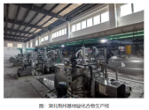
- Full control from raw material purification to compound and semiconductor-grade product manufacturing
- Diversified portfolio including bismuth metal materials (needles, beads, powders), compounds (hydroxide, oxychloride, citrate), and advanced semiconductor materials (oxide, sulfide, targets)

Applications span semiconductors (varistors, TEC coolers), photovoltaics, pharmaceuticals, and new energy.
Production bases are progressing:
- Wuhe (Anhui) & Qingyuan (Guangdong): formal production launched
- Jingzhou (Hubei) & Quzhou (Zhejiang): new capacity under promotion
Planned to complete expansion by end of 2025; expected to lead in annual output and sales volume.
Equipment Business: Domestic Substitution Accelerates
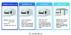
Subsidiary Kaishitong continues to lead the domestic ion implanter market with key milestones:
- Delivered 8 new 12-inch ion implanters, including first acceptance of a low-energy, high-beam implanter for CIS device doping, solving dark current issues and closing a critical domestic gap.
-Over 40 devices delivered since 2020, covering advanced logic, storage, power devices, and image sensors (CIS).
-Safe production volume exceeds 5 million 12-inch wafers, validation of large-scale reliability and transition from prototype to commercial deployment.
-Safe production volume exceeds 5 million 12-inch wafers, validation of large-scale reliability and transition from prototype to commercial deployment.

R&D focus on 28nm+ processes, including:
- Multi-electrode beam extraction
- Ultra-low energy beam transmission
- Vacuum isotropic mechanical scanning with high-precision angle control
Supply chain localization is advancing, core components (electrostatic chucks, flow meters) now increasingly sourced domestically, reducing overseas reliance and improving cost stability.
