Chinese semiconductor thread II

Michael90

Junior Member
Registered Member
More like they realized the software would just be pirated instead.
Not really. It’s just a matter of time, they will reinstate those measures in future and even more. It’s Just a seizefire not end of hostilities. As long as China keeps growing then you can’t expect the US is remain indifferent. Lol so if Chinese companies relying on US tech get complacent then they will only have themselves to blame when US cut off their technology again
lol
 

daifo

Major
Registered Member
People in Trumps administration like the AI czar David Sacks have publicly state that is better to get the Chinese industry dependent on US software and hardware to prevent the rise of local industries and also to use the sanction card. The Chinese industry needs to take it as a temporary reprieve rather than a long term solution.
 

tokenanalyst

Brigadier
Registered Member
More like they realized the software would just be pirated instead.

People in Trumps administration like the AI czar David Sacks have publicly state that is better to get the Chinese industry dependent on US software and hardware to prevent the rise of local industries and also to use the sanction card. The Chinese industry needs to take it as a temporary reprieve rather than a long term solution.
China exports controls on rare earths is hitting harder than most of the stooges in D.C. expected.
 

tokenanalyst

Brigadier
Registered Member

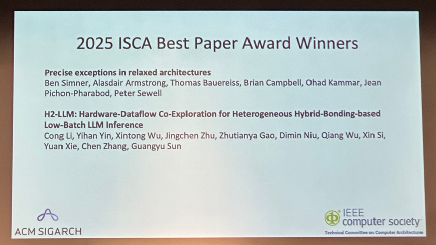
Peking University team won the ISCA Best Paper Award, breaking through the bottleneck of DRAM near-memory computing architecture for edge-side LLM​

Sun Guangyu's team at the School of Integrated Circuits at Peking University has made important breakthroughs in the DRAM near-memory computing architecture for accelerating edge-side large language model (LLM) reasoning. Based on a hybrid bonding process, the team developed the H2-LLM architecture, which effectively solved the problem of limited computing power of traditional DRAM near-memory computing architecture on edge devices. H2-LLM proposed a general near-memory computing architecture template and a "data-centric" data flow abstraction, and developed a design space exploration framework, achieving a 2.72-fold performance improvement and a 1.48-fold energy efficiency improvement compared to the baseline architecture.

38edf6029daf5b9c891400519a23886e.png

LLM has become one of the most influential technological breakthroughs in the field of artificial intelligence. With its powerful language understanding and generation capabilities, LLM has demonstrated outstanding performance in a variety of tasks such as problem reasoning, chat assistants, and code completion. With the widespread application of large language models, how to achieve efficient large language model reasoning on edge devices and provide a smooth user experience while meeting user needs such as personalized customization and data privacy has become an important issue that needs to be solved in the deployment of large language models.
This research is the result of industry-university-research cooperation between Peking University, Shanghai Jiao Tong University, Southeast University, Houmo Intelligence and Alibaba Damo Academy. It was published at the 52nd International Symposium on Computer Architecture (ISCA) and won the Best Paper Award. This is the first time that a domestic academic institution has won this honor at ISCA.

Please, Log in or Register to view URLs content!
 

tokenanalyst

Brigadier
Registered Member

The first equipment of Xiamen Silan Microelectronics' 8-inch silicon carbide power device chip manufacturing production line project (Phase I) was moved in ahead of schedule​

According to the official microblog of China Construction Third Engineering Bureau No. 1 Company, on June 26, the first equipment of Xiamen Silan Microelectronics' 8-inch silicon carbide power device chip manufacturing production line project (Phase I) undertaken by China Construction Third Engineering Bureau No. 1 Company was moved in ahead of schedule. The project is a key construction project of Fujian Province and Xiamen City in 2025 and is also the largest silicon carbide project in Xiamen.

The project is located in Xiang'an District, Xiamen City, Fujian Province, with a planned total construction area of 234,500 square meters. It is positioned as an 8-inch SiC power device manufacturing platform with international advanced level.

After the project is completed and put into production, it will significantly enhance Silan Microelectronics' production capacity and technical capabilities in the field of silicon carbide chip manufacturing, further consolidate its strategic position in China's third-generation semiconductor industry chain, and will also become one of the core supporting projects for Xiamen City to build the "Southeast Semiconductor Valley".

Chen Yue, secretary of the board of directors and vice president of Silan Microelectronics, said that their first phase project with a total investment of 7 billion yuan will make every effort to achieve initial production by the end of this year, put it into production in the first quarter of next year, and finally form an annual production capacity of 420,000 8-inch SiC power device chips by the end of 2028.

Please, Log in or Register to view URLs content!
 

tokenanalyst

Brigadier
Registered Member
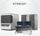
EBeam Lithography is being taking more seriously in China after being neglected for years.​

Jinjing Technology's electron beam exposure machine leads to new breakthroughs in domestic substitution of key core technologies, and the process of manufacturing graphics on photoresist is independently controllable!​


At the 2025 Zhongguancun Forum National Major Scientific Research Achievements Demonstration and Application Matchmaking Conference , The General Manager of Beijing Jinjing Technology, introduced Jinjing Technology 's technological research and development and industrialization achievements. The electron beam exposure machine product is independently developed by Jinjing Technology and relevant domestic advantageous institutions. Its functional configuration and core technical indicators are comparable to international first-class products, filling the gap in the commercialization of electron beam exposure machines in China. The product has entered the small-scale production stage, helping to solve the urgent needs of many heavyweight users, and has been delivered to users in small batches. It provides "root technology" support for China's cutting-edge science and technology fields such as quantum technology, nanotechnology, semiconductor microelectronics, and integrated circuits, and realizes the use of domestic scientific instruments to solve major basic scientific problems and help overcome difficulties in major technologies and engineering.

1751561325746.png

The electron beam exposure system is an important basic equipment for making micro-nano-sized graphic structures. It uses a focused electron beam to directly write on the surface of a sample coated with a photosensitive material (usually a photoresist), thereby manufacturing fine structures at the micron or nanometer level. The electron beam exposure system has the advantages of high resolution, precise control and high automation, and is widely used in the preparation of integrated circuits, photonic components (devices) and other micro-nano structure manufacturing fields.

Electron beam exposure refers to the process of using a focused electron beam to create patterns on photoresist, which is an extended application of photolithography. The electron beam exposure system is the hardware platform for implementing electron beam exposure technology. The performance of the system determines the key dimensions, splicing and overlay accuracy of the exposure process.

Jinjing Technology has achieved technological breakthroughs in the electron beam exposure process and core components of the equipment, and has taken the lead in launching the independently innovative, quality-controlled, and high-performance electron beam exposure system in China: Pharos 310. Many key technical indicators of the equipment have reached the world-class level, achieving the development goal of domestic substitution and independent control of electronic exposure equipment.


Please, Log in or Register to view URLs content!

Please, Log in or Register to view URLs content!
 

tokenanalyst

Brigadier
Registered Member

Breaking through the "bottleneck" dilemma of high-end transmission electron microscopes! BoZhong Instruments' 200kV field emission commercial product is officially released​

On June 28, Suzhou Bozhong Instrument Technology Co., Ltd. (hereinafter referred to as "Bozhong Instrument") successfully held the launch conference of the first domestically produced commercial 200kV field emission transmission electron microscope (TEM) at Bozhong Technology Park in Wujiang Economic and Technological Development Zone. The event was themed "Mirror World" and systematically presented the development process of domestic transmission electron microscopes from technical breakthroughs to industrialization through three chapters: "Breaking Boundaries and Sounding", "Establishing New Things and Observing Microscopy", and "Gathering Strength and Sailing Far". More than 100 representatives from government agencies, universities, research institutes, industry, finance, and media gathered at the scene to witness the "highlight moment" of innovation and development in the field of high-end scientific research instruments in China.

The core performance is benchmarked against the international advanced level.

Scientific and technological innovation and industrial innovation are the basic paths to developing new productivity. To develop new productivity, both scientific and technological innovation and industrial innovation are indispensable. Only by achieving deep integration can we promote revolutionary technological breakthroughs.

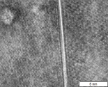
In the second chapter of this event, the first domestically produced commercial 200kV field emission transmission electron microscope, "BZ-F200", was officially released.

The first commercial 200kV field emission transmission electron microscope in China independently developed by BoZhong Instruments has broken through the technical bottleneck of "creating something from scratch" and simultaneously opened up the path for industrialization.
1751562067863.png

Tang Aiquan, general manager of BoZhong Instruments, gave a detailed introduction to the research and development process of the product to the guests present.

"After five years of technical research and repeated refinement, from the whole machine product to every key component, BoZhong Instruments has firmly grasped the core technology of the entire chain in its own hands." Tang Aiquan introduced that with the application of BZ-F200 transmission electron microscope in materials science, life science, semiconductor and other fields, it will effectively form new formats, new models and new kinetic energy, and become an important engine for cultivating and developing new quality productivity. In the future, BoZhong Instruments will firmly focus on the core technology of electron beam, continuously improve the product line, and empower the construction of industrial ecology by providing electron beam technology applications and services to the industry, and hand in the "BoZhong answer sheet" for the era proposition of China's high-tech self-reliance.

Please, Log in or Register to view URLs content!
 
Top