You are using an out of date browser. It may not display this or other websites correctly.
You should upgrade or use an alternative browser.
You should upgrade or use an alternative browser.
Chinese semiconductor thread II
- Thread starter vincent
- Start date
Design and implementation of high-precision online measurement system for ArF excimer laser pulse parameters
Institute of Microelectronics, Chinese Academy of SciencesUniversity of Chinese Academy of Sciences
Beijing Keyi Hongyuan Optoelectronic Technology Co., Ltd.
summary
Maintaining the stability of laser light source output energy is a key link in lithography, and it is necessary to perform high-precision online measurement of deep ultraviolet excimer light source pulse parameters. Traditional excimer laser energy measurement devices mostly work at low repetition rates. Aiming at the measurement requirements of high repetition rate excimer laser pulses, a laser pulse parameter online measurement system is designed. The peak holding circuit is used in conjunction with an analog-to-digital converter to achieve pulse energy acquisition. By establishing and simulating the parasitic equivalent model of the peak holding circuit, the design method of the high repetition rate excimer laser pulse peak holding circuit is optimized. The designed system is tested on a 193 nm ArF excimer light source platform, and the online extraction of excimer light source pulse parameters and real-time high-precision energy measurement are realized. After testing, when the light source is at a frequency of 6 kHz, the average relative error of the system energy measurement value relative to the standard energy meter is 0.22%, the maximum relative error is 0.56%, and the linearity is 99.83%, which is a useful exploration for the practical application of the online high-precision measurement system of deep ultraviolet excimer light source pulse parameters in lithography.
Ah OK so they want to handle the entire world market over to Deepseek by literally giving the rest of the world including extremely pro US but nonwhite countries only 7% of computational resources.
I was surprised to see that Israel was put into Tier 2. I would have expected Tier 1 or even an Israel-only "Tier 0.5" or "Tier 0."
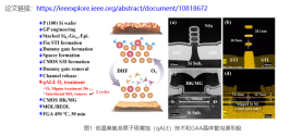
The Institute of Microelectronics successfully developed a GAA transistor that is close to an ideal switch using a new stacked nanosheet channel surface treatment technology.
The stacked nanosheet all-around gate (GAA) transistor has excellent gate control characteristics, higher driving performance and more circuit design flexibility. It is the core transistor structure after FinFET in mainstream integrated circuit manufacturing. At present, semiconductor giants such as Samsung Electronics (Samsung), TSMC (TSMC) and Intel (Intel) have or are about to adopt this device for mass production at 3 nanometers and below technology nodes. However, the stacked nanosheet GAA devices reported so far have a large channel interface state and are difficult to achieve ideal subthreshold switching. A key reason is that the newly introduced GeSi/Si superlattice stack at the material interface is easily affected by the integrated thermal budget, resulting in the diffusion and redistribution of Ge atoms, resulting in trace Ge atoms remaining on the surface after the nanosheet channel is released, causing additional interface defects and reduced carrier conductivity.
In response to this challenge, the IC Pioneer Process R&D Team of the Institute of Microelectronics proposed a low-temperature ozone quasi-atomic layer etch (qALE) technology that is fully compatible with the GAA transistor nanosheet channel release process. After the nanosheet channel is released, this technology achieves precise removal of Ge atoms remaining on the surface of the nanosheet channel through an extremely thin layer of ozone self-limited oxidation and corrosion reaction, avoiding damage to the inner Si channel. The characteristics of the developed CMOS device show that after low-temperature qALE treatment, the interface state density of the nanosheet channel is reduced by two orders of magnitude, the transistor subthreshold switch swing is optimized to 60.3 mV/dec, which is almost close to the device thermodynamic theoretical limit (60mV/dec), and the leakage current (I off ) is reduced by 66.7%. At the same time, due to the significant reduction in carrier scattering caused by the surface charge of the channel after treatment, the transistor on-state current (I on ) is also increased by more than 20%. This research work provides an efficient and low-cost technical path for the preparation of high-performance stacked nanosheet GAA devices.
The paper based on this research result, "Record 60.3 mV/dec Subthreshold Swing and >20% Performance Enhancement in Gate-All-Around Nanosheet CMOS Devices using O3-based Quasi-Atomic Layer Etching Treatment Technique" (doi:10.1109/LED.2024.3524259), was recently published in IEEE Electron Device Letters and successfully selected as the cover paper of the journal (Figure 3). Graduate students Jiang Renjie and Sang Guanqiao from the Institute of Microelectronics are the first authors of the paper, and researchers Zhang Qingzhu and Yin Huaxiang are co-corresponding authors. This research was supported by the Strategic Priority Research Program (Class A) of the Chinese Academy of Sciences and the National Natural Science Foundation of China.

60-90WDesign and implementation of high-precision online measurement system for ArF excimer laser pulse parameters
Institute of Microelectronics, Chinese Academy of Sciences
University of Chinese Academy of Sciences
Beijing Keyi Hongyuan Optoelectronic Technology Co., Ltd.
summaryMaintaining the stability of laser light source output energy is a key link in lithography, and it is necessary to perform high-precision online measurement of deep ultraviolet excimer light source pulse parameters. Traditional excimer laser energy measurement devices mostly work at low repetition rates. Aiming at the measurement requirements of high repetition rate excimer laser pulses, a laser pulse parameter online measurement system is designed. The peak holding circuit is used in conjunction with an analog-to-digital converter to achieve pulse energy acquisition. By establishing and simulating the parasitic equivalent model of the peak holding circuit, the design method of the high repetition rate excimer laser pulse peak holding circuit is optimized. The designed system is tested on a 193 nm ArF excimer light source platform, and the online extraction of excimer light source pulse parameters and real-time high-precision energy measurement are realized. After testing, when the light source is at a frequency of 6 kHz, the average relative error of the system energy measurement value relative to the standard energy meter is 0.22%, the maximum relative error is 0.56%, and the linearity is 99.83%, which is a useful exploration for the practical application of the online high-precision measurement system of deep ultraviolet excimer light source pulse parameters in lithography.
Dumb questions but are there any hyper specialized semiconductor chips that can only be by US companies? (Fabbing included).
I just rewatched old TV series and some of the plots include some ultra-specifics timing chips made for US military munitions.
I just rewatched old TV series and some of the plots include some ultra-specifics timing chips made for US military munitions.
Magnetic Pumps for Semiconductor Equipment.
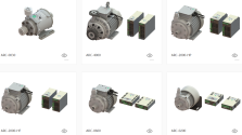
The ARC maglev-pump system is a revolutionary centrifugal pump that has no bearings to wear out or seals to break down and fail. Based on the principles of magnetic levitation, the pump's impeller is suspended contact-free, inside a sealed casing and is driven by the magnetic field of the motor. The impeller and casing are both fabricated from chemical-resistant high purity fluorocarbon resins. Together with the rotor magnet they make up the pump head. Fluid flow rate and pressure are precisely controlled by electronically regulating the impeller speed without pulsation. Closed loop flow or pressure control is easily configurable with the usage of an additional pressure or flow sensor.
The ARC series magnetic levitation pump system is a revolutionary centrifugal pump that has no bearing wear or seal failure. Based on the principle of magnetic levitation, the pump's impeller is suspended contactlessly in a sealed housing and is driven to rotate by the motor's magnetic field. Both the impeller and the housing are made of high-purity fluororesin that is resistant to chemical corrosion. Together with the rotor magnet, they form the pump head. Fluid flow and pressure can be precisely controlled by continuously adjusting the impeller speed through an electronic speed regulator to ensure there is no pulsation. Closed-loop flow or pressure control can be easily configured by using additional pressure or flow sensors. With the maturity of technology and applications, magnetic levitation pumps have been widely used in multiple processes in semiconductor manufacturing, such as electronic chemical liquid delivery, photolithography processing, silicon wafer etching, silicon wafer cleaning, metal plating and CMP liquid delivery.

The ARC series magnetic levitation pump system is a revolutionary centrifugal pump that has no bearing wear or seal failure. Based on the principle of magnetic levitation, the pump's impeller is suspended contactlessly in a sealed housing and is driven to rotate by the motor's magnetic field. Both the impeller and the housing are made of high-purity fluororesin that is resistant to chemical corrosion. Together with the rotor magnet, they form the pump head. Fluid flow and pressure can be precisely controlled by continuously adjusting the impeller speed through an electronic speed regulator to ensure there is no pulsation. Closed-loop flow or pressure control can be easily configured by using additional pressure or flow sensors. With the maturity of technology and applications, magnetic levitation pumps have been widely used in multiple processes in semiconductor manufacturing, such as electronic chemical liquid delivery, photolithography processing, silicon wafer etching, silicon wafer cleaning, metal plating and CMP liquid delivery.

Probably there are some designs and semiconductor manufacturing process recipes for some niche products that are only used in the US by NASA and/or US military, maybe some ASICs, hardrad chips, RF chips. Ironically this specialty chips don't require state of the art semiconductor facilities, probably more exoctic semiconductor materials like (GaAS, GaN, AlN), machines like MBE and exotic designs than EUV machines or 3nm etchers.Dumb questions but are there any hyper specialized semiconductor chips that can only be by US companies? (Fabbing included).
I just rewatched old TV series and some of the plots include some ultra-specifics timing chips made for US military munitions.
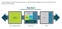
Skywater is one producer of these chips.
But the same goes to China.



Magnetic Pumps for Semiconductor Equipment.
View attachment 148954
The ARC maglev-pump system is a revolutionary centrifugal pump that has no bearings to wear out or seals to break down and fail. Based on the principles of magnetic levitation, the pump's impeller is suspended contact-free, inside a sealed casing and is driven by the magnetic field of the motor. The impeller and casing are both fabricated from chemical-resistant high purity fluorocarbon resins. Together with the rotor magnet they make up the pump head. Fluid flow rate and pressure are precisely controlled by electronically regulating the impeller speed without pulsation. Closed loop flow or pressure control is easily configurable with the usage of an additional pressure or flow sensor.
The ARC series magnetic levitation pump system is a revolutionary centrifugal pump that has no bearing wear or seal failure. Based on the principle of magnetic levitation, the pump's impeller is suspended contactlessly in a sealed housing and is driven to rotate by the motor's magnetic field. Both the impeller and the housing are made of high-purity fluororesin that is resistant to chemical corrosion. Together with the rotor magnet, they form the pump head. Fluid flow and pressure can be precisely controlled by continuously adjusting the impeller speed through an electronic speed regulator to ensure there is no pulsation. Closed-loop flow or pressure control can be easily configured by using additional pressure or flow sensors. With the maturity of technology and applications, magnetic levitation pumps have been widely used in multiple processes in semiconductor manufacturing, such as electronic chemical liquid delivery, photolithography processing, silicon wafer etching, silicon wafer cleaning, metal plating and CMP liquid delivery.
View attachment 148955

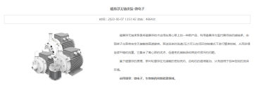
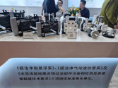
Ultra Clean Magnetic Levitation pumps for semiconductor equipment and immersion Lithography
you should learn more about it, these engineers have enough experience to fight with big companies... even though it is established less but... this company's experience is not inferior to companies with many years of experienceSiCarrier was founded in 2021. Naura is more a 15 years old. Experience matters in this industry. It's the difference between Intel and TSMC and ASML and Nikon,Canon.

