Chinese semiconductor thread II

tokenanalyst

Brigadier
Registered Member
ASML admitting that transistor scaling may have reached its limits and Advance Packaging is the future.​

ASML: 3D integration will become an increasingly important complementary technology to 2D shrinking​


According to media reports, on March 5, ASML released its 2024 annual report. CEO Christophe Fouquet said that if looking at ASML's future growth, lithography technology will undoubtedly remain one of the main driving forces of Moore's Law, and he believes that this will remain true for many years to come.
At the same time, 2D shrink is becoming increasingly difficult. This is not entirely due to the limitations of lithography<Bullshit>, but because we are almost reaching the limits of the transistors used by our logic and memory customers. To continue to make progress in 2D shrinking, innovations are needed in architecture and devices. This means 3D front-end integration, which will bring growth opportunities - because 3D integration technology relies on bonding, which in turn requires holistic lithography. "I think 3D integration will become an increasingly important complementary technology or technology combination to 2D shrinking," emphasized Christophe Fouquet.

Please, Log in or Register to view URLs content!
 

Hyper

Junior Member
Registered Member
ASML admitting that transistor scaling may have reached its limits and Advance Packaging is the future.​

ASML: 3D integration will become an increasingly important complementary technology to 2D shrinking​


According to media reports, on March 5, ASML released its 2024 annual report. CEO Christophe Fouquet said that if looking at ASML's future growth, lithography technology will undoubtedly remain one of the main driving forces of Moore's Law, and he believes that this will remain true for many years to come.
At the same time, 2D shrink is becoming increasingly difficult. This is not entirely due to the limitations of lithography<Bullshit>, but because we are almost reaching the limits of the transistors used by our logic and memory customers. To continue to make progress in 2D shrinking, innovations are needed in architecture and devices. This means 3D front-end integration, which will bring growth opportunities - because 3D integration technology relies on bonding, which in turn requires holistic lithography. "I think 3D integration will become an increasingly important complementary technology or technology combination to 2D shrinking," emphasized Christophe Fouquet.
Please, Log in or Register to view URLs content!
As I have said before. Lithography is about to reach its limits. One and half decades of shrink remaining. After that true 3D IC.
 

sunnymaxi

Major
Registered Member
The Sai Micro MEMS project is pretty important for all the sensor related stuff China needs actually.

Note, the comment about RF filters and MEMS Gallium Nitride chips. That's very interest.

I've not heard about that until now. Here is an article on GaN based MEMS resonator
Please, Log in or Register to view URLs content!

more research on this
Please, Log in or Register to view URLs content!
these two recent developments from Zhejiang University and Wuhan Uni

Zhejiang University researcher Ke Xugang's team released the third-generation semiconductor gallium nitride high-efficiency intelligent power supply chip for high-power AI data centers​


Please, Log in or Register to view URLs content!
--------------------------------------------------------------

Wuhan University, iGaN Laboratory of USTC and Institute of Electronics of MIIT have made new progress in the research of channel temperature monitoring of GaN-based HEMTs​


Please, Log in or Register to view URLs content!
 

tokenanalyst

Brigadier
Registered Member

16 new innovative enterprise headquarters were added in Pudong, including IC companies such as Will and Shengmei​


Recently, the awarding ceremony for the second batch of innovative enterprise headquarters in Shanghai was successfully held, and a total of 49 companies won this honor.

Among them, 16 enterprises in Pudong New Area were selected, covering multiple strategic emerging fields such as integrated circuits, biomedicine, artificial intelligence, etc. So far, Pudong New Area has a total of 29 innovative enterprise headquarters.

It is understood that among the Pudong New Area enterprises selected this time, enterprises in the field of integrated circuits are particularly eye-catching. Shanghai Will Semiconductor Co., Ltd., Unisoc (Shanghai) Technology Co., Ltd., ACM Semiconductor Equipment (Shanghai) Co., Ltd., VeriSilicon Microelectronics (Shanghai) Co., Ltd. and Shanghai Zhaoxin Integrated Circuit Co., Ltd. are all on the list. These enterprises have a leading position in integrated circuit design, manufacturing and equipment supply, and have made important contributions to promoting the development of the integrated circuit industry in Shanghai and even the whole country.
1. Integrated Circuit Field

Unisoc (Shanghai) Technology Co., Ltd.
ACM Semiconductor Equipment (Shanghai) Co., Ltd.
Montage Technology Co., Ltd.
VeriSilicon Microelectronics (Shanghai) Co., Ltd.
Shanghai Will Semiconductor Co., Ltd.
Shanghai Zhaoxin Integrated Circuit Co., Ltd.
Shanghai Jingce Semiconductor Technology Co., Ltd.
Shanghai Silicon Technology Co., Ltd.
Shanghai Feikai Materials Technology Co., Ltd.
Shanghai Fuhan Microelectronics Co., Ltd.

Please, Log in or Register to view URLs content!
 

tokenanalyst

Brigadier
Registered Member

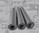
Analysis of the performance of high-strength silicon nitride ceramic tube against ion bombardment​

Hangzhou Haihe Precision Ceramics

In cutting-edge fields such as nuclear energy, semiconductor ion implantation, and space propulsion, the bombardment of high-energy ion beams places almost stringent requirements on material performance - resistance to radiation damage, high temperature resistance, thermal shock resistance, and low gas release rate are all essential. Traditional metal materials (such as stainless steel and molybdenum alloys) are difficult to cope with due to problems such as radiation swelling and sputtering contamination, while high-strength silicon nitride (Si₃N₄) ceramic tubes are reshaping the performance boundaries of ion beam equipment with their intrinsic radiation resistance, structural stability, and functional designability. This article deeply analyzes the scientific value and industrial potential of this material from four dimensions: material properties, anti-bombardment mechanism, engineering verification, and technological breakthroughs.

1741297344810.png

1. Intrinsic properties of silicon nitride ceramic tubes against ion bombardment

1. Extreme mechanical performance support​
  • High strength and toughness synergy: Silicon nitride ceramic tubes prepared by hot isostatic pressing (HIP) process have a bending strength of 800-1200 MPa and a fracture toughness of over 6.5 MPa·m¹/² (ordinary alumina ceramics are only 4 MPa·m¹/²), and can withstand micro-area stress concentration caused by ion bombardment.​
  • Fully densified structure: porosity <0.5%, eliminating nucleation sites for irradiation-induced voids and reducing volume expansion caused by ion implantation.​
  • Ultra-low thermal expansion coefficient (3.0-3.9×10⁻⁶/℃): Excellent matching with metal flange components to avoid sealing failure caused by thermal cycles.​
2. Microscopic mechanism of resistance to radiation damage​
  • Covalent bonds resist delocalization damage: The strong Si-N covalent bond energy of silicon nitride (~4.5 eV) is significantly higher than that of metal bonds (such as Fe-Fe bonds ~1.5 eV), and higher energy ions are required to induce lattice delocalization, thereby reducing the irradiation defect density.​
  • Self-healing grain boundary structure: The nanograin boundary glass phase (thickness <5 nm) formed by the Y₂O₃-Al₂O₃ sintering aid can absorb the vacancy clusters generated by irradiation and inhibit crack propagation.​
  • Low sputtering yield: The sputtering yield of silicon nitride surface is 2-3 orders of magnitude lower than that of molybdenum, reducing material loss and vacuum contamination caused by ion bombardment.​
Application of vacuum chamber in semiconductor ion implanter

In the 28 nm process boron ion implantation equipment, the silicon nitride ceramic tube continuously operated for 5,000 hours at 10⁻⁶ Pa vacuum and 500°C, with the surface metal contamination concentration <1×10¹⁰ atoms/cm², meeting the ultra-clean process requirements. Its dielectric strength (17.7 kV/mm) can effectively isolate the interference of high-voltage accelerating electric fields.
Application in Plasma etching equipment

Resistance to Cl₂/CF₄ plasma erosion: In a 300 mm wafer etching chamber, the life of silicon nitride tubes is 4 times that of aluminum oxide tubes, and there is no fluoride volatilization pollution.
RF matching characteristics: The dielectric constant (ε=6-8) has excellent matching with vacuum, reducing RF power reflection loss.

Please, Log in or Register to view URLs content!
 

tphuang

General
Staff member
Super Moderator
VIP Professional
Registered Member
these two recent developments from Zhejiang University and Wuhan Uni

Zhejiang University researcher Ke Xugang's team released the third-generation semiconductor gallium nitride high-efficiency intelligent power supply chip for high-power AI data centers​


Please, Log in or Register to view URLs content!
--------------------------------------------------------------

Wuhan University, iGaN Laboratory of USTC and Institute of Electronics of MIIT have made new progress in the research of channel temperature monitoring of GaN-based HEMTs​


Please, Log in or Register to view URLs content!
I don't believe those are MEM related.

GaN in power supply sector have been in use for a while now.

so this GaN MEM is a pretty big deal here.
 

gelgoog

Lieutenant General
Registered Member
Lithography is about to reach its limits. One and half decades of shrink remaining. After that true 3D IC.
They went from planar to vertical transistors. But they are still electronic devices which store electrons. Eventually they will hit a limit. Perhaps it will be necessary to move to photons or use some different paradigm.

The problem with 3D IC is the cooling. While it is possible to use a "layered cake" with some kind of dissipation pipes in between compute layers it will be difficult to get that to work.

One way to lower heat will be to further decrease clockspeed while increasing parallelism. The human brain is one example only runs at a couple hundred Hz and is water cooled.
 

OptimusLion

Junior Member
Registered Member
Key technologies for mass production of high-end semiconductor photomasks

Huazhong University of Science and Technology has the core technology to establish a mass production line for semiconductor masks at the 180 nm technology node; it has the ability to develop, design and verify semiconductor masks from 130 nm to 28 nm. The main research results are as follows: The team has mastered the core technology for mass production of mask MEMS micro-nano processing, such as the matching and optimization of various technical parameters of MEMS micro-nano processing processes such as electron beam lithography, laser lithography and nanoimprint lithography, as well as the rapid processing and compensation of large amounts of data with software.

Please, Log in or Register to view URLs content!
 

OptimusLion

Junior Member
Registered Member
Another Pan-semiconductor project settled in Optics Valley

Zhuoci Technology Co., Ltd. (hereinafter referred to as "Zhuoci Technology") signed a contract with the East Lake High-tech Zone to implement the Wuhan R&D and Production Base Project of Zhuoci Technology in Optics Valley. Zhuoci Technology was established in 2021 and focuses on the R&D and production of ceramic components in the pan-semiconductor field. It is currently a star startup in this field.

Its products have entered domestic first-class manufacturers such as Huawei and are widely used in semiconductors, display panel equipment, etc., with semiconductor business accounting for about 80%. The signed project is located in the East Lake Comprehensive Bonded Zone. Zhuoci Technology will invest in setting up a subsidiary in the Central China region to produce core components such as electrostatic chucks and ceramic heaters to serve Wuhan and surrounding wafer manufacturers.


092908291.png

Please, Log in or Register to view URLs content!
 
Top