Chinese semiconductor thread II

tokenanalyst

Brigadier
Registered Member

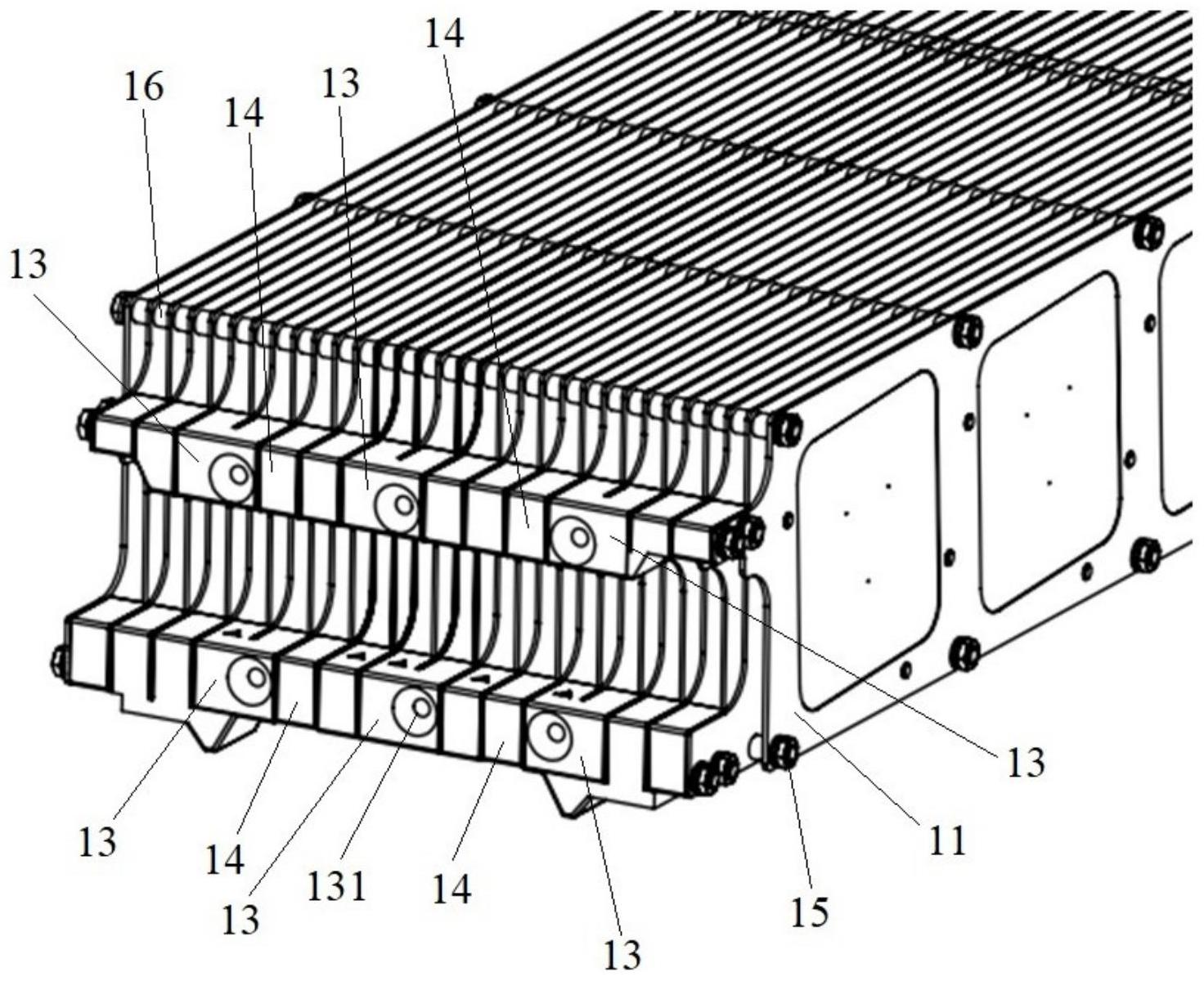
NAURA's "Crystal Boat and Semiconductor Process Equipment" Patent Announced​


Tianyancha shows that the patent of "Jingzhou and Semiconductor Process Equipment" of Beijing North Huachuang Microelectronics Equipment Co., Ltd. was announced. The application publication date is October 29, 2024, and the application publication number is CN118866781A.
1071737257619.0411.png

The present invention provides a wafer boat and semiconductor process equipment, the wafer boat includes a plurality of boat pieces for carrying wafers, the plurality of boat pieces are arranged in parallel and at equal intervals, the plurality of boat pieces are divided into a plurality of sections, each section includes a plurality of boat pieces, the boat pieces in different sections are insulated from each other, each section has a connection hole electrically connected to a radio frequency adjustment component, the boat pieces in different sections can be electrically connected to a radio frequency source through different radio frequency adjustment components, and the electrode polarities of the electrical connections of adjacent boat pieces are opposite. The wafer boat and semiconductor process equipment provided by the present invention can improve the uniformity of the coating thickness of a plurality of wafers in the same process.

Please, Log in or Register to view URLs content!
 

tokenanalyst

Brigadier
Registered Member

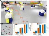
The Institute of Microelectronics has made new progress in the exploration of memristor neural-fuzzy hardware and applications.​


With the growing demand for high-performance neural networks, neural-symbolic artificial intelligence is attracting more and more attention due to its high interpretability and adaptability. It can enhance the reasoning and generalization of deep learning through symbolic knowledge, showing superior capabilities over deep learning. However, due to the complexity of symbolic knowledge representation and computation, designing and implementing efficient neural-symbolic hardware still faces many challenges such as computing power and energy efficiency.

Recently, the team led by Academician Liu Ming from the Key Laboratory of Integrated Circuit Manufacturing Technology of the Institute of Microelectronics proposed a solution for symbolic knowledge representation based on memory crossbar arrays. They demonstrated and verified the application of memristor neuro-fuzzy hardware systems in unsupervised, supervised and transfer learning tasks for the first time, providing guidance for the implementation of other knowledge-based technologies. The team directly represented the symbolic knowledge in the form of fuzzy logic and rules with the topological structure of the memory crossbar array, and used the intrinsic randomness of the memristor device to enhance the robustness of knowledge representation and improve the reasoning performance of the system. In order to solve the problem of slow convergence speed and poor effect of hardware in-situ training, the team first proposed a hybrid in-situ training technology under the framework of software and hardware collaborative optimization, which effectively reduced the problem of cumulative errors in the calculation process. The energy efficiency of the developed memristor neuro-fuzzy computing hardware exceeds that of FPGA by more than two orders of magnitude, and the energy consumption is only about one percent of that of ASIC. Taking robot navigation as an example, the neuro-fuzzy hardware shows superior adaptability to unknown environments. Compared with deep learning methods, the system learning speed is increased by about 6.6 times and the learning error rate is reduced by about 6 times. This work fully demonstrates the great potential of memristor neuromorphic computing systems in the field of artificial intelligence.

1732891643160.png1732891666904.png

Please, Log in or Register to view URLs content!
 

tokenanalyst

Brigadier
Registered Member

With a total investment of about 10 billion yuan, the Zhuhai Yiyuan Semiconductor Materials Industrial Base project started​


Recently, the groundbreaking ceremony of Zhuhai Yiyuan Semiconductor Materials Industrial Base Project (hereinafter referred to as "Yiyuan Semiconductor Project") was held in Jinwan District. The project has a total investment of about 10 billion yuan, focusing on the production of advanced materials in the upstream of the semiconductor industry chain, mainly producing synthetic quartz components and silicon carbide power module substrates with global leading process technology levels.

Beijing Eswin Technology Group Co., Ltd. is a leading domestic provider of integrated circuit products and services. Its core businesses include new-generation computing architecture chips and solutions based on RISC-V, 12-inch electronic-grade silicon wafers, and integrated circuit ecosystem development.

The Yiyuan Semiconductor project that started construction this time was incubated by the ecological chain development business unit of Eswi Group and strategically led by Huafa Group. It is a semiconductor material industry base integrating R&D, production and sales built by both parties in Jinwan District. It is an important layout in the key links of the upstream of the semiconductor industry chain and is also Zhuhai’s first 10 billion-level investment project in 2024.

Please, Log in or Register to view URLs content!
 

tokenanalyst

Brigadier
Registered Member

ACM Shanghai launches three new panel-level advanced packaging products​


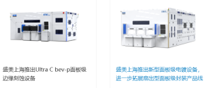
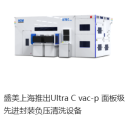
According to reports, Shengmei Shanghai recently stated on its investor interaction platform that in the third quarter, the company launched three new panel-level advanced packaging products, including horizontal electroplating equipment, edge etching equipment and negative pressure cleaning equipment.

Shengmei Shanghai said that its panel-level advanced packaging technology can be applied to micron-level high-density packaging, especially suitable for GPU applications in AI packaging and high-density HBM. The company's 600mm×600mm and 515mm×510mm panel-level advanced packaging can solve the problem of limited area and high cost of AI chips in 300mm silicon wafer packaging. Currently, many of the world's leading semiconductor manufacturers have chosen it as an AI chip packaging solution.
1732893450958.png1732893468862.png

Please, Log in or Register to view URLs content!
 

Randomuser

Senior Member
Registered Member
But now Samsung AI chips are banned by China anyway, since China is making its own chips.
Even if let's say one day TSMC, Samsung etc all have no more China limits, it's will be too late to stop what's happening. There's already a lot of development in local Chinese manufacturers and once they feel confident using their products, it's gonna be difficult to tell China to go back. Especially when they know such limits could be put back anytime.
 

tokenanalyst

Brigadier
Registered Member

A filtering device for photoresist production and processing​

Nantong Co ltd

CN118904084A​

Abstract​

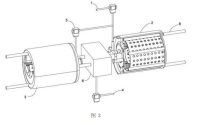
The invention discloses a filtering device for photoresist production and processing, comprising a first filtering module and a second filtering module. The photoresist solution is circulated and filtered N times between the first filtering module and the second filtering module, N is an integer greater than or equal to 2, and an adjustable filter membrane is arranged in the first filtering module and the second filtering module. After the N times of filtering, the photoresist solution is led out from the photoresist output end, and an adjustment mechanism can change the pore size of the adjustable filter membrane. When N times of filtering are performed, it is only necessary to change the pore size of the adjustable filter membrane in the first filtering module and the second filtering module in turn, and keep the photoresist solution circulating between the first filtering module and the second filtering module. Compared with the traditional multi-stage filtration, it does not need to realize multiple devices in series, and the filtering level can be adaptively adjusted, thereby improving the utilization rate of the filtering device.​

1732902457405.png1732902431070.png
 

tphuang

Lieutenant General
Staff member
Super Moderator
VIP Professional
Registered Member
very interesting article here on DDIC pricing and foundry.

Please, Log in or Register to view URLs content!

Not a surprise to us that follow this, but Mainland foundry capacity and share will grow significantly over next 2 years, especially from SMIC, Nexchip and HH. It will overtaken Taiwan in production
 

tokenanalyst

Brigadier
Registered Member
Improve grating sensors for lithography​

Homodyne grating displacement measurement system and photolithography machine dual worktable system.​

CN118670268A​

Abstract​

The present invention relates to the technical field of ultra-precision displacement measurement, and provides a homodyne grating displacement measurement system and a photolithography machine double worktable system. By integrating a light emitting component and a photoelectric acquisition card in a laser light source device, and arranging the laser light source device on a coarse motion table, the output laser, the reception of return light, and the photoelectric conversion acquisition functions can be integrated, and the layout design of the existing laser light source cabinet placed under the elevated floor can be replaced, so as to improve the integration of the worktable, shorten the transmission distance of the optical fiber, improve the laser utilization rate of the system, achieve high measurement accuracy, and make the system more concise and the structure more compact, solve the problems of optical fiber disturbance, low transmission efficiency, and laser safety, so as to achieve the function of realizing high-precision position measurement in an extremely short optical path, and reduce the difficulty of subsequent maintenance and repair.​

1732909328734.png
 

tokenanalyst

Brigadier
Registered Member

With an investment of RMB 7.38 billion, the first phase of Anjieli Meiwei's high-end packaging substrate project was completed and put into production​

Xiamen Industry and Information Technology, the first phase of the high-end packaging substrate and high-end HDI production capacity construction project of Xiamen Anjieli Meivi Technology Co., Ltd. has been completed and put into trial operation.
It is reported that the project is located in the Integrated Circuit Manufacturing Industrial Park in Haicang District. It is planned to build a production base integrating R&D, high-tech intelligent manufacturing, sales and services, with a total area of about 194,000 square meters and a planned total construction area of about 400,000 square meters. The project is expected to have a total investment of 7.38 billion yuan and will be built in two phases. The core product line of the first phase of the project mainly focuses on FC-BGA, including production plants, R&D centers and other necessary supporting facilities, with a total construction area of about 220,000 square meters.

Please, Log in or Register to view URLs content!
 

tokenanalyst

Brigadier
Registered Member

China's integrated circuit output increased by 24.8% from January to October, and exports increased by 11.3% year-on-year​


The integrated circuit output reached 353 billion pieces, a year-on-year increase of 24.8%. From January to October, exports reached 246 billion pieces, a year-on-year increase of 11.3%.
In terms of economic benefits, the electronic information manufacturing industry above designated size achieved operating income of 12.96 trillion yuan, a year-on-year increase of 7.2%, of which the total profit reached 514.9 billion yuan, a year-on-year increase of 8.4%. The operating income profit margin was 4.0%, an increase of 0.1 percentage point from January to September.
In addition, the investment growth of the electronic information manufacturing industry from January to October was also very prominent, with fixed asset investment increasing by 13.2% year-on-year, 0.9 and 4.4 percentage points higher than the investment growth rates of industry and high-tech manufacturing in the same period, respectively. This investment growth trend indicates that my country's integrated circuit industry will continue to expand its scale and enhance its R&D and production capabilities to meet the needs of domestic and foreign markets. This not only provides a strong impetus for the growth of my country's electronic information manufacturing industry, but also contributes to the stability and development of the global semiconductor supply chain.

Please, Log in or Register to view URLs content!
 
Top