Chinese semiconductor thread II

tokenanalyst

Brigadier
Registered Member

CNNC successfully mass-produced the world's first X/γ nuclear radiation dose detection chip​


On October 25, China National Nuclear Corporation (CNNC) announced yesterday that the world's first X/γ nuclear radiation dose detection chip developed by the Nuclear Safety and Environmental Engineering Technology Institute of CNNC Institute of Atomic Energy has been successfully put into mass production.

The chip has a range of 100nSv/h (nanosievert/hour)-10mSv/h (millisievert/hour) for X/γ-ray dose rate, and a detectable energy range of 50keV (kiloelectronvolt)-2MeV (megaelectronvolt). Its size is only 15mm×15mm×3mm, and it can operate in a temperature range of -20℃~50℃, while also having an ultra-low power consumption of 1mW (milliwatt). Although it is "small and exquisite", the sensitivity of this chip is comparable to that of the Geiger-Muller counter tube used for conventional environmental measurements.

Users only need to carry out simple secondary development based on the chip data manual and it can be applied to radiation dose monitoring scenarios such as radiation workplaces, personnel, and environments in the nuclear field.

It is reported that the chip adopts a standardized interface design and can be used as a universal radiation sensor device. It is suitable for reflow soldering and can be quickly integrated into various smart equipment such as mobile phones, tablets, smart helmets, drones, etc. It can be used to develop smart terminal products with radiation detection functions.

Please, Log in or Register to view URLs content!
 

tokenanalyst

Brigadier
Registered Member

Jingga Semiconductor enters the new generation semiconductor public service platform project​

According to Qilu Evening News, the Jinan Semiconductor and Aerospace Information Industry High-Value Technology Achievement Transformation Matchmaking Conference was successfully held at the National Supercomputing Jinan Center in Licheng District recently. At the conference, 12 projects from Jinan Licheng Digital Technology Group Co., Ltd., Jinan Jinggu Research Institute and other units were signed.

Shandong Jinggai Semiconductor Co., Ltd. has settled in the new generation semiconductor public service platform project. It will rely on the latest GaN single crystal growth and substrate processing technology achievements developed by the National Key Laboratory of Crystal Materials and the Institute of New Generation Semiconductor Materials of Shandong University to carry out the research and development, production and sales of third-generation semiconductor material gallium nitride (GaN) single crystal substrates, which can provide basic support for multiple industries such as electronics, communications, and computing, and help shape the core competitiveness of the industry.
 

tokenanalyst

Brigadier
Registered Member

Lithography Equipment manufacturer SVG Optronics increased their revenue in 2024Q3​


announced its 2024 third-quarter report. Data showed that the company achieved operating income of 1.395 billion yuan in the first three quarters of 2024, a year-on-year increase of 11.25%; net profit attributable to shareholders reached 39.3688 million yuan, a year-on-year increase of 204.97%, continuing the growth momentum in the first half of the year. The pace of performance growth accelerated and continued to advance rapidly in the third quarter

At the same time, the company's overseas business expansion has achieved remarkable results. Among them, the flexible transparent conductive material business continued to expand overseas customers during the reporting period, driving revenue to increase by approximately RMB 30.752 million, a year-on-year increase of approximately 27.08%; the nano-texture material business benefited from its application in the global main models of a certain international leading European automobile brand, with revenue increasing by approximately RMB 27.9404 million, a year-on-year increase of approximately 656.68%. With the increase in subsequent application brands and models, the scale of revenue is expected to further expand.

In terms of new micro-nano materials in the fields of consumer electronics and automobiles, the light-guiding materials business continued to adjust its revenue structure, increasing the proportion of high-gross-profit businesses and turning losses into profits year-on-year; the flexible transparent conductive materials business also saw a significant year-on-year increase in gross profit margin as the yield rate increased and the business direction was optimized.

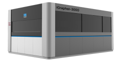
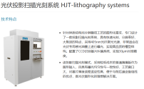
Lithography equipment is expected to usher in an explosion in the fourth quarter of this year, Suzhou Dawei's micro-nano optical high-end equipment mainly includes two product lines: laser direct writing lithography equipment and nanoimprint lithography equipment, all of which are independently developed, designed and produced by the company. Through continuous equipment iteration and upgrading over the years, a modular, knowledge-intensive, upgradeable and rapidly configurable micro-nano manufacturing platform has been gradually built, providing core technical support for the development and maintenance of technology and products.
In the direct writing laser lithography equipment market, although the global market is dominated by European and American manufacturers, Suzhou Dawei Ge has achieved a certain degree of fame and market share in the domestic scientific research field with its unique writing mode and large-format micro-nano 3D structure preparation capabilities, and has gradually attracted the attention of corporate customers. At present, the company's direct writing laser lithography equipment has been sold to some leading companies in the industry, and the company is also actively expanding the application of direct writing lithography in the field of semiconductor masks and IC substrates.
1729884751304.png
As one of the first companies in China to realize the industrialization of nanoimprint technology, Suzhou Weige's nanoimprint lithography equipment is widely used in the manufacture of micro-nano optical materials, naked-eye 3D displays, AR waveguides and other optical components, and closely follows the development trend of international nanoimprint technology. In addition, the company is actively exploring the application prospects of nanoimprint in cutting-edge fields such as microfluidics, biochips and integrated circuit manufacturing.
1729884821991.png


There is no doubt that lithography equipment is a strategic focus of Su Dawei's business. In recent years, the company has been increasing its sales of lithography equipment. In 2023, sales revenue of various types of equipment increased by 266.71% year-on-year to 31.9115 million yuan; in the first quarter of 2024, sales increased by approximately 9 million yuan year-on-year, an increase of approximately 277.11%.​

Please, Log in or Register to view URLs content!
 

tokenanalyst

Brigadier
Registered Member

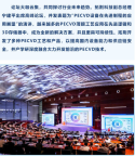
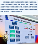
Looks like Piotech is going full force into Hybrid Bonding. Piotech and UPrecision Hybrid Bonding push could significantly benefit China HBM, 3D-NAND, 3D IC, Chiplet and 3D-DRAM developments​


Tuojing Technology brought its PF-300M PECVD (Plasma Enhanced Chemical Vapor Deposition product series) and Bonding (wafer-to-wafer hybrid bonding) equipment models to the Bay Core Exhibition, and competed with the industry Colleagues share Tuojing’s latest technological breakthroughs and innovations. The gorgeous and smart design of Tuojing's booth became the highlight of this exhibition. The products and designs attracted a large number of visitors to stop and communicate, bringing new vitality and thinking to this exhibition.

1729886414238.png1729886234789.png

Please, Log in or Register to view URLs content!
 
Last edited:

gotodistance

New Member
Registered Member

TSMC's Arizona Plant and US Chip Ambitions​

TSMC has achieved early production yields at its first plant in Arizona that surpass similar factories back home, a significant breakthrough for a US expansion project initially dogged by delays and worker strife. Anja Manuel, executive director of the Aspen Strategy Group and former diplomat, joins Caroline Hyde and Ed Ludlow to discuss what that means for the US's chip manufacturing ambitions on "Bloomberg Technology."


ansy1968

Brigadier
Registered Member
ASML CEO: China Might be Able to Produce 5nm and 3nm Chips amid U.S. Export Restrictions

Please, Log in or Register to view URLs content!
Yes, 5nm is a given with current DUVi SMIC have, 3NM is in the works in 2025 when the expected Chinese EUVL makes its appearance, these 2 nodes are expected since Liang Mong Song announced it in his resignation letter back in 2020. What I'm interested is what follow next? Will they forgo the 2nm node and go directly to Graphene chip? or other means like 3D chip stacking. I think the use of silicon had reach its limit and having 7nm , 5nm and 3nm tech node is enough to power the Chinese tech industry until the end of this decade.

Liang Mong Song: SMIC's 7nm node has already completed full development, and is preparing for mass production in April 2021. Designs and most of the development for 5nm and 3nm nodes have also already been completed, only awaiting EUVL delivery at this point.​


latenlazy

Brigadier
Yes, 5nm is a given with current DUVi SMIC have, 3NM is in the works in 2025 when the expected Chinese EUVL makes its appearance, these 2 nodes are expected since Liang Mong Song announced it in his resignation letter back in 2020. What I'm interested is what follow next? Will they forgo the 2nm node and go directly to Graphene chip? or other means like 3D chip stacking. I think the use of silicon had reach its limit and having 7nm , 5nm and 3nm tech node is enough to power the Chinese tech industry until the end of this decade.

Liang Mong Song: SMIC's 7nm node has already completed full development, and is preparing for mass production in April 2021. Designs and most of the development for 5nm and 3nm nodes have also already been completed, only awaiting EUVL delivery at this point.​

“Graphene” or “3D stacking” doesn’t mean there isn’t a process node size or that the node size doesn’t matter.
 

BlackWindMnt

Captain
Registered Member
Yes, 5nm is a given with current DUVi SMIC have, 3NM is in the works in 2025 when the expected Chinese EUVL makes its appearance, these 2 nodes are expected since Liang Mong Song announced it in his resignation letter back in 2020. What I'm interested is what follow next? Will they forgo the 2nm node and go directly to Graphene chip? or other means like 3D chip stacking. I think the use of silicon had reach its limit and having 7nm , 5nm and 3nm tech node is enough to power the Chinese tech industry until the end of this decade.

Liang Mong Song: SMIC's 7nm node has already completed full development, and is preparing for mass production in April 2021. Designs and most of the development for 5nm and 3nm nodes have also already been completed, only awaiting EUVL delivery at this point.​

Yeah it seems with silicon the cap seems to be 5ghz clockspeeds under usable workload. Maybe with new materials we can get to 10, 100ghz etc with acceptable power usage. That would be a world altering level of development.
 
Top