Chinese semiconductor thread II

tokenanalyst

Brigadier
Registered Member
Man the level of precision and mechanical stability you would need to get alignments consistently right at the single nanometer level is *insane*.
Well alignment and overlay are use differently in projection lithography, alignment is between the mark and the mask and overlay is between different layers across the process, IDK how that would be for NIL but assuming because the absence of masks, overlay and alignment would be close related:

-An Overlay of 20nm if can be keep along the process would be like KrF level precision, good for 180-110 nm process or for metal layers.
-An Overlay of 10nm would be dry ArF precision good for backend processes and 65nm+ process
-An Overlay of 3nm would be close to Immersion and EUV, at that point because the resolution of NIL is near perfect, the sky would be the limit.
 

tokenanalyst

Brigadier
Registered Member
just a simple question bro,

Can Qingdao Tianren Micro Nano Tech Co., Ltd beat Canon in NIL Litho machines and solve problems you mentioned above, if they continue to put efforts in R&D ??
Yes, I think the are trying to get into the plausible MRAM memory market pretty much like Canon is pushing their system on NAND and DRAM. So is very probably than Tenren Nano would also push for that market.

"Obtained some representative work in key processes of micro-nano processing technology/ultra-precision manufacturing equipment and ultra-high density magnetic storage:

1) 7nm node extreme ultraviolet (EUV) lithography technology exposure agent research and development, 7nm Node/13nm period EUV interference lithography (IL) process, Si 3 N 4 mask manufacturing process for EUV/X-ray array technology;

2) Use EUVIL to prepare the smallest 20nm two-dimensional lattice that can be obtained by optical methods for the next generation of magnetic recording media;

3) 8/12-inch next-generation Sub-20nm spin transfer torque magnetic random access memory chip STT-MRAM process (comparable to the best Samsung process technology), 50nm resolution, 1:7.5, the world’s highest aspect ratio structure The 8/12 -inch nanoimprint equipment is used in the magnetic sensor array process;

4) Cooperate with GermanLitho/Tianren Micro-Nano Technology and Leuven Instrument industry-university-research institute to jointly develop special equipment focusing on magnetic sensor array/MRAM 2/4/6/8-inch nanoimprinting and 8/12-inch RIE/IBE dual engraving Etching technology exclusive etching equipment for magnetic materials.

If Canon NIL systems become popular every fab manager China and their grandmothers are going to look to China NIL companies for solutions.
 

tokenanalyst

Brigadier
Registered Member
Wanye Enterprise promoting domestic Hydrogen Implanters.

Towards full coverage of product lines, and playing the role of "chain leader" in the industry

"The current stage is relatively difficult for Kaishitong, and the R&D investment is much higher, but the gap between us and the international advanced is constantly narrowing, the performance of the original products is constantly improving, and the new product lines are constantly being supplemented, and full coverage is about to be achieved." Li Yongjun said.

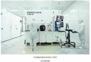
In March of this year, Kaishitong's independently developed and produced new CIS low-energy large-beam ion implanter has been moved into the customer's production line, becoming the first domestic equipment supplier in China to receive an order for CIS low-energy large-beam ion implanter.

1727475436528.png

At present, Kaishitong is actively benchmarking the new demands and applications of the development of the domestic integrated circuit industry, aiming at the evolution trend of cutting-edge integrated circuit processes, seizing the opportunity of localization, and promoting the implementation of special process equipment including SOI hydrogen ion implanters, medium-beam ion implanters, and ultra-high-energy ion implanters, and accelerating the research and development and application of SiC compound semiconductor ion implanters for special processes.

The breakthrough of complete equipment is closely related to the coordinated development of the industrial chain. Kaishitong plays an indispensable role as a "chain leader" and actively promotes the localization process of parts. It is gratifying that many key parts projects have been successfully borne fruit. As Dr. Li Yongjun said, Kaishitong is committed to leading upstream component companies to achieve integrated development through collaborative innovation and in-depth cooperation between industry, academia and research, and helping downstream users to cope with the challenges of continuity in local chip manufacturing. After continuous efforts, a supply chain system with resilience and diversity has been initially formed, and the independent and controllable supply chain of domestic ion implanters is about to become a reality. In the future, Kaishitong will continue to deepen its research and development and innovation in ion implanters, and strive to become a name card in the field of high-end equipment manufacturing.

Please, Log in or Register to view URLs content!
 

OptimusLion

New Member
Registered Member
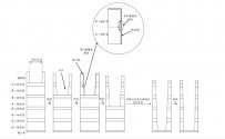
NAURA's patent for "an etching method, semiconductor process equipment and computing equipment" was published

Tianyancha shows that Beijing North Huachuang Microelectronics Equipment Co., Ltd.'s "An Etching Method, Semiconductor Process Equipment and Computing Equipment" patent was announced, the application publication date is September 6, 2024, and the application publication number is CN118610121A. The embodiment of this specification provides an etching method, which forms a protective film on the surface of the film layer structure to be etched through a deposition step, and the protective film can fill the damaged part of the opening side wall to improve the flatness of the opening side wall.

Please, Log in or Register to view URLs content!

IMG_20240929_081647_912.jpg
 
Top