Chinese semiconductor thread II

interestedseal

Junior Member
Registered Member
Crazy!, do you think it will get to the smartphone in the next 5 years? .... imagine, how big the photo size would be, currently is already too big with "only" Samsung 50MP ... which is totally unnecessary
Please, Log in or Register to view URLs content!

Please, Log in or Register to view URLs content!


Yeah 600MP sounds totally unnecessary for consumer grade cameras. They are targeting lensless microscopy, remote sensing and machine vision markets
 

OppositeDay

Senior Member
Registered Member
Crazy!, do you think it will get to the smartphone in the next 5 years? .... imagine, how big the photo size would be, currently is already too big with "only" Samsung 50MP ... which is totally unnecessary

My mom has a Sony A7r4. Its full frame 61MP sensor is often limited by lens. Decent modern primes weighting around half a kilo are often not sharp enough to fully take advantage of the sensor's resolution. A full frame sensor is 7 times the size of a 1-inch sensor typically used for premium phones. So no there's just no point in super high resolution for phone cameras.
 

tokenanalyst

Brigadier
Registered Member

The Industrial Research Institute (Yantai) Semiconductor Display Photolithography Special Light Source Industry Incubation Project was officially signed​


On August 9, the Industrial Research Institute (Yantai) successfully signed the semiconductor display lithography special light source industry incubation project. With professional project management and efficient and high-quality services, the Industrial Research Institute (Yantai) promoted the establishment and development of Shandong Industrial Research Yuandian Optoelectronics Technology Co., Ltd. in Yantai, adding impetus to the high-level development of the optoelectronic industry chain .

The project company is committed to developing and producing a series of products with high-power ultra-short arc lamps as the core, and taking into account other low-power special industry light source products. These innovative products are designed to fill the key technology gap in the field of semiconductor display special lithography light sources in China, and are expected to play a key role in many cutting-edge technology fields such as semiconductor lithography and display panel manufacturing.

At the project signing ceremony, the project leader solemnly promised to promote the project implementation with high standards and strict requirements, devote efforts to rigorous project management and continuous technological innovation, and actively move towards the goal of becoming an industry-leading enterprise.

The successful signing of the project symbolizes that the Institute of Industrial Technology (Yantai) has taken solid steps in exploring new business models. Taking this new starting point as an opportunity, the Institute of Industrial Technology (Yantai) will continue to rely on its own advantages to screen and cultivate a number of projects with high technological content, huge development potential, good market prospects, strong innovation capabilities and high industrialization maturity.

Please, Log in or Register to view URLs content!
 

tokenanalyst

Brigadier
Registered Member

China Builds "Sapphire Wafers" to Improve Efficiency​


A team of Chinese scientists has made a significant stride in chip technology by developing dielectric wafers made of artificial sapphire. Their groundbreaking research, published in Nature on Wednesday, lays a crucial foundation for the development of more power-efficient chips.

As electronic devices continue to shrink and demand higher performance, the miniaturization of transistors has presented challenges, especially in the realm of dielectric materials.

These materials typically act as insulators in chips, but their effectiveness diminishes at the nanoscale – that's one of the reasons our smartphones tend to heat up and have short battery life.

To address this issue, the researchers at the Shanghai Institute of Microsystem and Information Technology, Chinese Academy of Sciences, created artificial sapphire dielectric wafers using a novel intercalation oxidation process.

"The aluminum oxide we created is essentially artificial sapphire, identical to natural sapphire in terms of crystal structure, dielectric properties and insulation characteristics," said Tian Zi'ao, a researcher involved in the project.

1723298148992.png

Please, Log in or Register to view URLs content!
 

tokenanalyst

Brigadier
Registered Member

Progress has been made in the research direction of fully automatic chip design​


Chip design is a very challenging, labor-intensive and resource-intensive task. Usually, a team of engineers needs to write code and then generate circuit logic with the help of electronic design automation (EDA) tools. For the manually written code, the engineering team needs to repeatedly perform functional verification and performance/power optimization on it. This process usually requires a team of hundreds of people to iterate for months or years to complete.

The goal of fully automated chip design is to have machines automatically generate circuit logic that meets functional and performance requirements, thereby greatly reducing manpower and resource investment and accelerating design iterations. Since A. Church, one of the founders of computer science, proposed the "Church problem" in 1957, fully automated design of processor chips has become a long-term vision in the field of artificial intelligence. However, due to the high accuracy requirements of processor chip circuits and the large design space, the processor logic must be logically designed by human experts. This has become a bottleneck in design efficiency in the entire process.

Led by Chen Yunji, director of the National Key Laboratory of Processor Chips, Institute of Computing Technology, Chinese Academy of Sciences, the team focused on solving the two major challenges of accuracy and scale faced by automatic design of processor chips, and proposed a verification-centered intelligent design methodology for processors: starting from random circuits, the machine automatically completes repeated iterations including verification, debugging, and repair until the target circuit that meets the design requirements is obtained.

Specifically, the team transformed the problem of automatic processor design into the problem of automatically generating a large-scale BDD (Binary Decision Diagram) representation from the input and output (IO) of the verification program. To address this problem, the team designed a binary guessing diagram (BSD), replacing the deterministic subgraph in the traditional BDD with the guessing nodes in the BSD determined by Monte Carlo sampling of IO. By continuously expanding and merging the BSD, the generated circuit can gradually approach the target circuit logic. The above method automatically designed a general-purpose processor with more than 4 million logic gates, Enlightenment No. 1, in 5 hours, which increased the scale of circuits that can be automatically designed by existing work by 3 to 4 orders of magnitude. The Enlightenment No. 1 chip is the world's first processor chip designed without human intervention and fully automatically. It can run the Linux operating system normally, and its measured performance reaches the level of Intel 486. The related paper Automated CPU Design by Learning from Input-Output Examples has been accepted by the CCF-A conference IJCAI 2024.

To further improve the performance of automatically generated processors, the team proposed an automatic pipeline design method based on gate-level dependency analysis. Data dependency analysis is the key to automatic pipeline design. Unlike traditional data dependency analysis, which can only be performed at high levels such as registers, this method automatically performs data flow analysis at the fine-grained gate circuit level. Based on the analysis results, a fine-grained pipeline control unit was constructed through a binary guessing graph. While ensuring the correctness of the function, the gate-level forward pass and guessing were used to improve the program execution efficiency, achieving a 1.57x performance improvement; more importantly, in some cases, a better pipeline design than human design can be found, with an average throughput improvement of 31%. The related paper Revisiting Automatic Pipelining: Gate-level Forwarding and Speculation has been accepted by the CCF-A conference DAC 2024.

Please, Log in or Register to view URLs content!
 

tokenanalyst

Brigadier
Registered Member

Creating a new benchmark for heterogeneous computing! Guoshu Jilian released the first CXL hybrid resource pool reference design​

Guosu Group released the industry's first CXL hybrid resource pool (Compute Express Link Hybrid Resource Pool) reference design. This reference design is the first CXL hardware device that supports heterogeneous computing architecture, marking a new stage of heterogeneous computing in the data center field for CXL technology.

Today, National Data Network, a leading high-speed interconnect chip and solution design company, released the industry's first CXL hybrid resource pool (Compute Express Link Hybrid Resource Pool, hereinafter referred to as "CHRP") reference design. This reference design is the first CXL hardware device that supports heterogeneous computing architecture, marking a new stage of heterogeneous computing in the data center field for CXL technology.

Based on the advanced features of FPGA and self-developed CXL protocol IP, Guosu Jilian can achieve the systematic integration of multiple heterogeneous resources such as CPU, GPU, DDR, SSD, FPGA, etc., providing an efficient and flexible acceleration platform for specific applications.

1723298820567.png

CHRP provides 8 PCIe AIC standard slots, which can flexibly connect CPU, GPU, DDR, SSD, FPGA and various acceleration cards to meet diverse workload requirements. The system provides up to 8 PCIe ASM interfaces to the outside, supporting up to 8 hosts to directly connect, and realize efficient sharing of heterogeneous resources. With the help of CXL hybrid resource pool, the host can transparently access the heterogeneous components in the resource pool, significantly improving the business processing speed and flexibility.

It is worth mentioning that CHRP can also exist as an independent host system, independently forming a heterogeneous system node to provide high-performance business processing capabilities for special services.

Guosu Jilian not only provides reference designs at the hardware level, but also provides dedicated drivers to ensure that the operating system can accurately identify hardware resources and achieve smooth system expansion.

Please, Log in or Register to view URLs content!
 

tokenanalyst

Brigadier
Registered Member

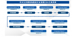
Leading universities and colleges have joined hands with well-known publishing institutions to launch a number of university textbooks based on the HuaDa Empyrean EDA platform​


Recently, HuaDa JiuTian, together with well-known Chinese publishing houses such as the Electronic Industry Press and the People's Posts and Telecommunications Press, launched two university textbooks based on the HuaDa JiuTian EDA platform. They are an important part of a series of domestic EDA university textbooks, which aims to further promote the cultivation of talents in China's integrated circuit industry and improve the level of teaching, training and scientific research in related fields.

Empyrean Analog Integrated Circuit Design and Engineering, edited by Professor Hu Yuanqi of the School of Integrated Circuit Science and Engineering of Beihang University, was officially published by Posts and Telecommunications Press. The monograph was selected into the special planning project of national key publications during the 14th Five-Year Plan period and the knowledge empowerment project of industry and information technology.

The IC design EDA platform used in the book is the Empyrean Aether® system, the full-process integrated circuit design platform of HuaDa Empyrean. During the writing of this book, HuaDa Empyrean provided a full range of university program software support and rich basic teaching cases, and the technical team also provided professional technical support and collaboration.​

1723305256057.png

Please, Log in or Register to view URLs content!
 

tokenanalyst

Brigadier
Registered Member

To solve the problem of ultra-large-scale design, Renesas decided to introduce Empyrean Skipper® from HuaDa Empyrean​


Beijing HuaDa Empyrean Technology Co., Ltd., a leading domestic EDA company, recently announced that Renesas Electronics Corporation (hereinafter referred to as "Renesas Electronics"), a leading global semiconductor solution provider, has introduced HuaDa Empyrean's Empyrean Skipper® tool as its layout management solution.

Empyrean Skipper® is suitable for viewing, analyzing and modifying IC layouts. It can read in ultra-large-scale chip data at high speed, maximizing the work efficiency of engineers. For ultra-large-scale chips using advanced processes, especially those in communications, HPC, and AI, layout data often reaches tens of GB or even hundreds of GB. In the later stages of chip design, layout data needs to be opened repeatedly for various inspections, analyses, and modifications. Previous tools would take tens of minutes or even hours to complete the reading, while Empyrean Skipper® can read in tens of GB of data in ten minutes, saving engineers valuable time.

“As design complexity increases, the size of chips is also growing. The time required to read in and analyze layout data has also increased significantly, consuming a lot of our engineers’ time. We expect Empyrean Skipper® to be a good solution to this problem.” Yukio Minota, Director of the Digital Backend Design Technology Department at Renesas Electronics, affirmed the excellent performance of Empyrean Skipper®.

Please, Log in or Register to view URLs content!
 
Top