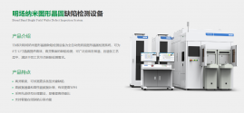
Tianjue Technology released the first 40nm bright-field nano-pattern wafer defect inspection equipment in China, opening a new era of domestic high-end semiconductor inspection equipment
his is another new phase of progress made by Tianjue Technology less than a year after it officially delivered the TB1000 , a wide-band bright-field defect inspection equipment for 12 -inch wafer 65~90nm technology nodes in August last year.

The Importance of High-Precision Brightfield Defect Inspection Equipment
From a whole wafer to a single chip, in addition to the well-known photolithography machine, a series of necessary production equipment is also required, including diffusion furnaces, etchers, ion implanters, thin film deposition equipment, chemical mechanical polishers and cleaning machines.
Defect detection equipment is an important tool to ensure chip quality, reduce production costs, and promote process iteration, and is indispensable in the chip production process. In particular, as the process continues to evolve, the cost of manufacturing chips is getting higher and higher, and the importance of detection equipment is increasing day by day. Among them, bright field defect detection equipment with higher detection accuracy and more comprehensive defect type coverage is highly favored by the industry.
As a representative of domestic semiconductor equipment manufacturers, Silicon Semiconductor, founded in November 2021, has brought together top talents from well-known domestic and foreign semiconductor equipment companies, wafer foundries, listed companies and research institutions, focusing on the research and development, production and sales of high-end wafer defect detection equipment and components, and striving to fill the gap in the domestic defect detection equipment market . Relying on an excellent technical team and advanced technical strength, it has gradually broken the monopoly of foreign companies such as KLA on the defect detection market, injecting new vitality into the development of the domestic semiconductor industry.
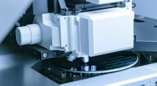
TB1500 is the latest research and development achievement of Silicon Semiconductor. All key components are independently controllable, and advanced signal processing algorithms are used to effectively improve the signal-to-noise ratio and detection sensitivity . In order to meet the process requirements of the 40nm technology node, TB1500 has improved the brightness and sensitivity of the light source, increased the field of view and speed of the objective lens, and can capture smaller defect sizes.


