Chinese semiconductor thread II

tphuang

Lieutenant General
Staff member
Super Moderator
VIP Professional
Registered Member
just curious, when could SMIC or Huawei ramp up its 7nm (5nm in the future) production so Huawei could cut prices? some posts mentioned 2nd of this year.

with both Apple and Nvidia offering big discounts in China now, I don't think Huawei's products are competitive with the discounted high-end products from Apple or Nvidia, unless you want to support "Made in China", personally I fail to see Huawei's products provide better values for the money?

Huawei is best stuck at 5nm for the foreseeable future unless domestic EUV comes out while Apple is moving into 2nm soon, as long as Apple is willing to cut prices, very hard for Huawei to beat Apple's value proposition.
I mean they are ramping up production quite a bit already.

Huawei chips are better than Nvidia that are available. Huawei phones are higher end than iPhone in terms of satcom support, photography, charging speed and other areas. Just exactly what makes you think Huawei phone cannot beat Apple's value proposition?
 

Phead128

Captain
Staff member
Moderator - World Affairs
with both Apple and Nvidia offering big discounts in China now, I don't think Huawei's products are competitive with the discounted high-end products from Apple or Nvidia, unless you want to support "Made in China", personally I fail to see Huawei's products provide better values for the money?
My wife ditched her iPhone 14 Pro for a Huawei Mate 60 Pro. The camera quality is excellent, she even prefers the camera quality for taking selfies vs. the iPhone 14 Pro.

I can personally tell you Mate 60 Pro is incredibly fast, there is no discernible difference in daily routine use between TSMC 4nm (A16 bionic) and SMIC 7nm (N+2) chips. Absolutely zero difference. You can even go down to 1.6nm, there is zero discernible difference in daily routine use.

Huawei already regained leadership in China and dethroned Apple to be the #1 mobile phone marketshare again.
 

ansy1968

Brigadier
Registered Member
My wife ditched her iPhone 14 Pro for a Huawei Mate 60 Pro. The camera quality is excellent, she even prefers the camera quality for taking selfies vs. the iPhone 14 Pro.

I can personally tell you Mate 60 Pro is incredibly fast, there is no discernible difference in daily routine use between TSMC 4nm (A16 bionic) and SMIC 7nm (N+2) chips. Absolutely zero difference. You can even go down to 1.6nm, there is zero discernible difference in daily routine use.

Huawei already regained leadership in China and dethroned Apple to be the #1 mobile phone marketshare again.
Lucky you, I hope my wife may do the same BUT knowing the power of American brand it will take a lot of convincing or maybe you may give some tips and I'm all ears bro. ;)
 

gotodistance

New Member
Registered Member
It's a trick!!!! 3nm, 5nm impossible? This is a very calculated action by the Huawei Cloud CEO, and it means that China can definitely achieve 3-nano and 5-nano.

Byeong-seo Jeon worked in Korea as a China and semiconductor expert in the securities industry for a long time and received a doctorate from Fudan University.

You will be able to understand it to some extent if you watch it with English subtitles.


tokenanalyst

Brigadier
Registered Member

Ultrasmooth Ti/Al multilayer with a Ti seed layer for EUV applications.​

Abstract​


Al-base multilayers have attracted much interest in the extreme ultraviolet (EUV) optics field, but high roughness of this multilayer due to the Al film is still a big concern. Here, a strategy of the seed layer was proposed to reduce the surface roughness and intermixing layer thickness of the Al-base multilayer. Ti film is not only a seed layer, but also an absorption layer in this novel multilayer. An optimized Ti/Al multilayer film structure was designed to work at 21.1 nm, while investigating the use of Ti as a seed layer to reduce the roughness and enhance the peak reflectivity. The experimental results showed that the Ti seed layer effectively reduced the surface roughness and intermixing layer thickness and improved the reflectance. At 21.1 nm, the peak reflectance reached 39.6%, with a bandwidth of only 1.0 nm and an RMS roughness of 0.17 nm. Ti/Al multilayer also exhibits good stability. This multilayer has potential application in high-precision optics, such as corona detection, which requires extreme low light scattering of multilayer mirror.

Please, Log in or Register to view URLs content!
 

tokenanalyst

Brigadier
Registered Member

Xinyuan Micro obtained a patent for semiconductor process equipment to achieve matching with various sources​


Tianyancha intellectual property information shows that Shenyang Xinyuan Microelectronics Equipment Co., Ltd. has obtained a patent called "A wafer carrier for semiconductor process equipment".

The patent abstract shows that the utility model belongs to the technical field of semiconductor process equipment, specifically, a wafer carrying device of semiconductor process equipment, including a bottom plate, a top plate, a side plate group and a support column group. The bottom plate, the top plate and the side plate group are connected to form a box structure, and each support column group is respectively arranged on the side plate of each side plate group. The height position of each support column of each support column group corresponds to the height position of each support column of the other support column groups. The utility model sets a plurality of support column groups in the box structure surrounded by the bottom plate, the top plate and the side plate, so that the wafer is supported by a plurality of support columns located at the same height position, which can greatly reduce the contact area with the wafer, effectively avoiding the problem that if there are burrs on the wafer or the edge is not chamfered, the wafer is easily stuck with the wafer carrying device when taking and placing the wafer, causing the wafer to break. It can adapt to the working conditions of diversified film sources and achieve matching with various forms of film sources.​
 

tokenanalyst

Brigadier
Registered Member
New product launch in Wuxi 2024

(1) Suzhou Xinrui Technology Co., Ltd. - Introduction to 12-inch bonding and debonding equipment

(2) Suzhou Ecoris Intelligent Equipment Co., Ltd. - Nano-scale chip-to-wafer high-precision hybrid bonding equipment

( 3) Shanghai Microelectronics Equipment (Group) Co., Ltd. - SOI800 series fully automatic optical defect detection equipment
(800 refer to SMEE ArF immersion lithography machines series) while the (600 series will stay as SMEE dry lithography machines)

(4) Wenxian Microelectronics Co., Ltd. - Automotive-grade high-side driver switches and energy chain semiconductor solutions

(5) Wuxi Yiwen Electronic Technology Co., Ltd. - third-generation semiconductor eight-inch thin film etching equipment

(6) Yanwei (Jiangsu) Semiconductor Technology Co., Ltd. - (High-yield) High-K ALD thin film deposition equipment

(7) Jiaxing Jingyan Intelligent Equipment Technology Co., Ltd. - High-density ultra-thin chip stacking die bonding machine

(8) Jiaxing Qingting Optoelectronics Co., Ltd. - Wirebond 3D AOI

(9) Shenyang Heyan Technology Co., Ltd. – Wafer grinding machine

(10) Ridong Intelligent Equipment Technology (Shenzhen) Co., Ltd. - IC bonding machine WBD2200 Plus

(11) Zhisiyuan Integrated Circuit Design (Wuxi) Co., Ltd. - medium and high voltage power supply and driver chips

(12) Jiangsu Leibo Microelectronics Equipment Co., Ltd. - New self-made Aligner lithography machine

(13) ACM Semiconductor Equipment (Shanghai) Co., Ltd. – Front-end coating and development Track equipment
(officially)

(14) Jiangsu Microguide Nanotechnology Co., Ltd. - iTomic® MW series batch atomic layer deposition coating system
(officially)

(15) Robei (Wuxi) Microelectronics Co., Ltd. – Independent and controllable high-performance general-purpose computing chips
 

tokenanalyst

Brigadier
Registered Member

Sanan Optoelectronics: Becoming a semiconductor company with international competitiveness​


Recently, a reporter from Shanghai Securities News visited Sanan Optoelectronics and learned that the company's 6-inch silicon carbide substrates have been shipped in batches to international customers; the 8-inch substrate epitaxial process has been debugged and samples have been sent to key overseas customers for verification, and the yield level of substrate products ranks among the best in the country and is steadily improving.

Lin Kechuang, vice chairman and general manager of Sanan Optoelectronics, revealed in an exclusive interview with a reporter that the company has more than 800 cooperation intentions and customers in the field of silicon carbide; after the project of Hunan Sanan reaches full production at the end of this year, the production capacity will be about 360,000 pieces/year, an increase of more than 50% over the current production capacity.

"From LED to compound semiconductor manufacturing, Sanan Optoelectronics has always focused on the industry's most cutting-edge technology research and application during more than 20 years of industrial upgrading." Lin Kechuan introduced that Sanan Optoelectronics has now formed four major business segments: LED, integrated circuit RF front-end, optical technology, and power electronics. The latest breakthrough in silicon carbide business is a microcosm of the company's dedication to developing new quality productivity.

Please, Log in or Register to view URLs content!
 

tokenanalyst

Brigadier
Registered Member

ACM Shanghai launches new product, wafer cleaning equipment with frame, upgrading advanced packaging product portfolio​


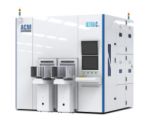
ACM Semiconductor Equipment (Shanghai) Co., Ltd. (hereinafter referred to as "ACM Shanghai"), a leading supplier of wafer process solutions for semiconductor front-end and advanced wafer-level packaging applications, today launched a wafer-on-frame cleaning system for advanced packaging. The equipment can effectively clean semiconductor wafers during the post-debonding cleaning process.
The innovative solvent recovery system of the framed wafer cleaning equipment has significant environmental and cost benefits. This function can achieve nearly 100% solvent recovery and filtration, thereby reducing the amount of chemicals used in the production process. ACM Shanghai has completed the installation and verification of the first cooperative equipment with a Chinese integrated circuit manufacturer.
Dr. Hui Wang, Chairman of ACM Shanghai, said: "ACM Shanghai has successfully promoted the continued development of advanced packaging with its rich industry experience and customer relationships. We believe that as the semiconductor industry shifts to advanced packaging and back-end 3D integrated design, our wafer-on-frame cleaning equipment will further attract various customer groups. We are committed to sustainable development and provide customers with equipment that recycles solvents, thereby reducing waste and lowering the total cost of ownership in the production process."
1718038926251.png
About Frame Wafer Cleaning Equipment
The framed wafer cleaning equipment is equipped with four chambers, and provides a variety of configurations through options such as high-purity solvents, MegPie solvents, deionized water, nano solvents and isopropyl alcohol (IPA) nozzles, which can be connected to adapt to various processes. The equipment can also complete the cleaning and drying processes in the same chamber at the same time to achieve efficient cleaning and drying; it is available in 8-inch and 12-inch configurations, suitable for standard wafers and framed wafers.
In addition, the equipment can seamlessly process standard wafers and framed wafers, and the configuration of the chamber and loading port can process two types of wafers at the same time, ensuring flexible and efficient operation capabilities. ACM Shanghai's self-developed processing technology enables the equipment to process thin wafers with a thickness of less than 150 microns. ACM's Smart Megasonix® technology (patent number: ZL200910050834.2) is used in the cleaning process to perform comprehensive and damage-free cleaning of the entire wafer. The equipment can efficiently remove photoresist, especially residues on the edges, to ensure that the surface of the wafer is smooth and residue-free after cleaning.

Technical advantages:
- Specially designed vacuum chucks reduce the possibility of damage to the back of the wafer, setting a new standard for precision under extreme cleaning conditions;
- Adopts a patented fixing method (patent application number: 202310787637.9) by ACM Shanghai to ensure excellent stability when handling framed wafers during high-speed rotation;
- With excellent anti-static performance, ion rods are used in the equipment front-end module (EFEM) and each chamber module, supplemented by a DI-CO2 mixer to protect the wafer from static electricity during the entire process.​

Please, Log in or Register to view URLs content!
 
Top