TSMC took 3 years to get from 5 nm to 3 nm.Compare to the progress of TSMC,it is slow
You are using an out of date browser. It may not display this or other websites correctly.
You should upgrade or use an alternative browser.
You should upgrade or use an alternative browser.
Chinese semiconductor thread II
- Thread starter vincent
- Start date
Whoever wrote this article is really ignorant about computer architecture and chips in general. I mean I am basically a software guy and even I know more about hardware architectures than these people.
Talk about counting your chickens before they hatched.
SMSC has much less fab capacity than TSMC. It is as simple as that. And they are not just producing chips for HiSilicon. We don't know the yield. Period. All we can make is some assumptions.
Qualcomm is still using the N4P process. It is like an N5 half-node. It is only Apple which is using the N3 process.it was still years behind other semiconductor manufacturers, which had moved on to 3nm-process chips. But they caught up faster than most expected.
Oh really? All I have read makes me think HiSilicon is following a tick-tock development model where they are trying out a new Taishan core design with the 9010 in the existing SMIC N+2 process, before the SMIC N+3 process comes out and they shrink it down.In the days that followed, we saw similar sentiments appear online. TechInsights suggested that the Kirin 9010 appeared to be on the same N+2 process node. The prevailing theory is that the Kirin 9010 is, at its heart, a 9000S with a revised design aimed at improving production yields. The improvements may not be limited to production though—early benchmarks suggest that the 9010 also performs a little better than the 9000S.
That's two nodes difference not three. And the TSMC N3 node has the same SRAM cell size as the N5.SMIC was unable to progress to the 5nm node process since the release of the 9000S while TSMC has an N2 node in its sights—a generational difference of 3 nodes representing six years of process refinement. That should put the technical challenges facing China’s semiconductor industry into perspective.
Talk about counting your chickens before they hatched.
So 8% more performance with same manufacturing process and a lower clockspeed is "marginally better". Right...Meanwhile, the performance increase between the 9000S and 9010 remains in single digits. This new SoC is marginally better but not the huge leap that was expected.
No you dolts. The Taishan cores have two-way simultaneous multi-threading (SMT). So it is one 2300 MHz Taishan core, and two 2180 MHz Taishan cores.To achieve those single-digit performance increases, the Kirin 9010’s 12-core SoC uses six ARM Cortex A510 efficiency cores running at 1550 MHz paired with four Taishan v121 cores running at 2180 MHz and two Taishan v121 cores running at 2300 MHz.
These people don't even know what SMT is and that the Kirin SoC's Taishan core has it.By comparison, the 9000S is reported to have an 8-core SoC (confusingly there are lots of benchmarks that report 12 cores ever since a recent HarmonyOS update but this is unlikely) containing four ARM Cortex A510’s running at 1530 MHz paired with three Taishan cores running at 2150 MHz and one Taishan v120 core running at 2620 MHz.
The Taishan cores are custom ARM compatible core designs by HiSilicon and they aren't ARM Cortex anything. Cortex is a trade name ARM Ltd. uses for their own core designs.The Taishan cores are custom ARM Cortex processors and the version numbers provide some insight into the revision number printed on the chip. The A510 itself is an ARM Cortex processor from 2020, since superseded by the A520.
If this was Apple and not Huawei these people would be passing the supply constraints as some sort of Apple victory meaning there is huge demand.the shortages and backlogs on orders for Huawei’s Pura 70 and even the months-old Mate 60 imply that, as analysts had predicted, the N+2 process does not produce sufficient yields to meet demand. This restricts SMIC’s ability to produce the 7nm Kirin 9000S and 9010 SoC’s in large enough quantities to meet demand.
SMSC has much less fab capacity than TSMC. It is as simple as that. And they are not just producing chips for HiSilicon. We don't know the yield. Period. All we can make is some assumptions.
DRAM manufacturers do not call their processes 7nm or 5nm. They use names like D1a. Reflective of it being some kind of 1x nm class process. As in ten something nanometer. These guys are really ignorant.This is where CXMT comes in. As China’s premiere DRAM fab, they’ve recently produced the first fully Chinese-manufactured LPDDR5 module which we expect to start seeing in the wild soon. However, DRAM also relies heavily on the latest node processes for performance and power efficiency. Again, as CXMT attempts to produce on 7nm and 5nm nodes, they will have to grapple with the problem of production yields dropping significantly.
It is impossible to know the yield given the information we have. But a cursory analysis by TechInsights looking at the roughness of the process features in the Kirin 9000S made them think the yields should be good.For now, the US has successfully restrained China’s ability to mass produce on the 7nm node at high yields.
No you dolts. It takes time to qualify a new process.By extension, it has also prevented China from mass producing on an N5 equivalent node at high yields.
Last edited:
Whoever wrote this article is really ignorant about computer architecture and chips in general. I mean I am basically a software guy and even I know more about hardware architectures than these people.
Agreed, this is a crappy article. I am the same, know next to nothing about hardware, but enough to know that that article was useless.
Firstly, the fact that there was any change AT ALL was a big thing since literally no one changes their chip twice in a year. That the chip was iterated upon to improve architecture, which improves both performance and power efficiency (and also yields??) is a BIG thing.
The only thing that I learned from this article was that DRAM was still SK Hynix, however in other teardowns that I have seen, the DRAM itself was unknown. Maybe they are using domestic DRAM in P70 Ultra?
Is it slow compared to UMC? Or global foundries?Compare to the progress of TSMC,it is slow
You are either just trolling again or purposefully disingenuous at best. Always putting out these crappy articles.
Did TSMC get from 7nm to 5nm in 6 months?Compare to the progress of TSMC,it is slow
Let us be fair. The articles he posts are not all like this. Most are pretty decent. But this one was really bad.You are either just trolling again or purposefully disingenuous at best. Always putting out these crappy articles.
All the work done by whoever did the teardown and captured the photos of the surface of the NAND chips was wasted by the really crappy analysis these people make.
The SMIC N+2 process has higher transistor density than either of the best TSMC or Intel DUV processes.Compare to the progress of TSMC, it is slow
To get to a higher density both TSMC and Intel ended up using EUV tools in some layers.
Is this considered bad? Because you can be pretty certain Intel tried to delay introduction of EUV as much as possible.
Intel used to be process leaders for decades. Gordon Moore was an Intel founder. And they were basically beaten by SMIC at their own game.
Last edited:
What's the story behind Intel nowadays? I've heard conflicting claims like some say they are still way behind while some say they're actually going to catch up with TSMC soon or somethingLet us be fair. The articles he posts are not all like this. Most are pretty decent. But this one was really bad.
All the work done by whoever did the teardown and captured the photos of the surface of the NAND chips was wasted by the really crappy analysis these people make.
The SMIC N+2 process has higher transistor density than either of the best TSMC or Intel DUV processes.
To get to a higher density both TSMC and Intel ended up using EUV tools in some layers.
Is this considered bad? Because you can be pretty certain Intel tried to delay introduction of EUV as much as possible.
Intel used to be process leaders for decades. Gordon Moore was an Intel founder. And they were basically beaten by SMIC at their own game.
They have the Intel 4 process. It is more like a Samsung 5nm than a TSMC 5nm process. It kinda sucks.What's the story behind Intel nowadays? I've heard conflicting claims like some say they are still way behind while some say they're actually going to catch up with TSMC soon or something
And Intel only started using it like 3 years later.
Intel 3 is supposed to come late this year. They have huge plans to do lots of process improvements in like half the time the industry normally takes to do such things. Like a process every year. We will see how successful they are at this.
Intel tried to stick with DUV for as long as they could. Tried to use a more complex scheme than SAQP and it failed.
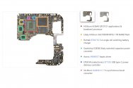
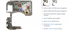
Picking some interesting part from the tear down's (just 2 pictures here, the others are on the link)


We can see that the only non mainland China suppliers are Taiwan's for battery charger, Bosch for accelerometer & gyroscope and SK Hynix for DRAM.
The RF front-end IC are marked HiSilicon, but it would be interesting to know who is the foundry and also who are the suppliers of the SAW/BAW filters, PA amplifiers and all the other front end analog stuff.
All in all an impressive supply chain engineering effort by Huawei. I'm not sure people understand what it means to raise a whole bunch of new suppliers to world-class flagship product level.
IMO this is the biggest contribution of Huawei to China.
Regarding memory, I don't fully buy this narrative of SK Hynix DRAM chips still from 2020 stockpile...anyhow I have no data here. I just have some doubts....maybe HW still has some old DRAM chip to use at product launch, when specialized firms get their sample to tear-down. I think we will hear more on that in the future...
Anyhow DRAM IC in this sample is confirmed to be like in the Mate 60, the H58GG6MK6G LPDDR5-6400, still not a LPDDR5X....we are well in CXMT territory. That SK Hynix chip can turn into a CXMT quite quickly if needed.
Regarding the tear-down, this firm IFixit, does not have the advanced instrumentation to perform a deep chip analysis at transistor level. That's why they have no clues about NAND and the other HiSilicon chips. TechInsights has the instrumentation, but for some reason their analysis has been classified.
Last edited:
