
Chinese semiconductor thread II

tokenanalyst

Lieutenant General
Registered Member

Peking University Team Achieves All-Carbon Nanotube CFET Digital Logic Circuit.​

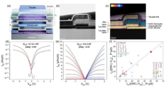
Researchers from Peking University, led by Professor Liang Xuelei, have achieved a major breakthrough in semiconductor technology by developing the world’s first digital logic circuit based on all-carbon nanotube complementary field-effect transistors (CFETs). As traditional silicon-based transistors near their physical scaling limits, the global industry has turned to CFET architecture a design that vertically stacks N-type and P-type devices to achieve higher transistor density for future sub-2-nanometer process nodes. Carbon nanotubes are especially well-suited for this approach due to their ultra-high carrier mobility, near-ballistic charge transport, and low-temperature processing compatibility, which is crucial for three-dimensional chip integration. This work fills a critical international research gap by demonstrating that carbon nanotube CFETs can transition from isolated components into fully functional digital systems, offering a viable pathway for post-silicon computing architectures.
1783958788410.png
The development faced two primary technical hurdles: balancing the inherently mismatched driving capabilities of P-type and N-type carbon nanotube transistors, and preventing high-temperature fabrication steps from degrading the performance of underlying device layers. To resolve these issues, the research team introduced a novel doping-free CMOS design strategy that optimizes transistor geometry to ensure matched electrical characteristics while thermally insulating lower layers during upper-layer processing. This innovative structural approach enabled the successful fabrication of highly stable all-carbon nanotube CFET inverters that operate reliably across a broad voltage range of 0.2 V to 1 V with low power consumption. At just 1 V, the devices achieved a peak voltage gain of 164, setting a new record for low-dimensional semiconductor CFETs and confirming their suitability for complex digital logic operations.

Building on these high-performance components, the team successfully integrated them into complete digital circuits, including basic AND, OR, NAND, and NOR gates, as well as a four-transistor static random-access memory (SRAM) cell. Most notably, they constructed the world’s first five-stage ring oscillator using this all-carbon nanotube CFET architecture, marking a decisive step from single-device validation to system-level implementation.
This milestone not only demonstrates the practical viability of carbon nanotube-based vertical stacking but also establishes a foundational blueprint for next-generation high-density, low-power integrated circuits that could ultimately overcome the limitations of traditional silicon technology.

Please, Log in or Register to view URLs content!
 

tokenanalyst

Lieutenant General
Registered Member

TCL CSOT's 27-inch printed OLED is about to enter mass production.​


TCL is accelerating its production process for medium and large-sized OLED displays. The high-end IT display market, including monitors, laptops, and tablets, is expected to undergo an inevitable shift in its landscape.

According to reports, TCL CSOT, a display subsidiary of TCL, has successfully completed internal verification and entered mass production of a 27-inch 4K 120Hz RGB striped OLED display panel developed using inkjet printing technology. This marks TCL's first independent production of medium-to-large-size OLED panels, excluding special-purpose displays such as those for medical applications.

TCL CSOT announced an investment plan of approximately RMB 1.5 billion, aiming to triple the production capacity of its Wuhan factory. The factory is expected to serve as a transitional and outpost base until the completion of its 8.6-generation OLED T8 inkjet printing production line under construction in Guangzhou.

This means that TCL will begin producing OLED panels ahead of schedule, before its 8.6-generation OLED factory, which is expected to achieve mass production in 2027. The market landscape in this field is expected to change rapidly.

Please, Log in or Register to view URLs content!
 

sunnymaxi

Colonel
Registered Member

Peking University Team Achieves All-Carbon Nanotube CFET Digital Logic Circuit.​

Researchers from Peking University, led by Professor Liang Xuelei, have achieved a major breakthrough in semiconductor technology by developing the world’s first digital logic circuit based on all-carbon nanotube complementary field-effect transistors (CFETs). As traditional silicon-based transistors near their physical scaling limits, the global industry has turned to CFET architecture a design that vertically stacks N-type and P-type devices to achieve higher transistor density for future sub-2-nanometer process nodes. Carbon nanotubes are especially well-suited for this approach due to their ultra-high carrier mobility, near-ballistic charge transport, and low-temperature processing compatibility, which is crucial for three-dimensional chip integration. This work fills a critical international research gap by demonstrating that carbon nanotube CFETs can transition from isolated components into fully functional digital systems, offering a viable pathway for post-silicon computing architectures.
View attachment 178111
The development faced two primary technical hurdles: balancing the inherently mismatched driving capabilities of P-type and N-type carbon nanotube transistors, and preventing high-temperature fabrication steps from degrading the performance of underlying device layers. To resolve these issues, the research team introduced a novel doping-free CMOS design strategy that optimizes transistor geometry to ensure matched electrical characteristics while thermally insulating lower layers during upper-layer processing. This innovative structural approach enabled the successful fabrication of highly stable all-carbon nanotube CFET inverters that operate reliably across a broad voltage range of 0.2 V to 1 V with low power consumption. At just 1 V, the devices achieved a peak voltage gain of 164, setting a new record for low-dimensional semiconductor CFETs and confirming their suitability for complex digital logic operations.

Building on these high-performance components, the team successfully integrated them into complete digital circuits, including basic AND, OR, NAND, and NOR gates, as well as a four-transistor static random-access memory (SRAM) cell. Most notably, they constructed the world’s first five-stage ring oscillator using this all-carbon nanotube CFET architecture, marking a decisive step from single-device validation to system-level implementation.
This milestone not only demonstrates the practical viability of carbon nanotube-based vertical stacking but also establishes a foundational blueprint for next-generation high-density, low-power integrated circuits that could ultimately overcome the limitations of traditional silicon technology.

Please, Log in or Register to view URLs content!
TSMC is targeting the CFET architecture for its sub-1nm logic nodes, aiming for commercial production around 2032–2033.

its good to see the progress in CFET architecture from top Chinese research institutes.
 

tokenanalyst

Lieutenant General
Registered Member

Another indium phosphide (IP) photonics chip company completes financing of over 100 million yuan.​


Recently, Changzhou Zhonglou Specialized and Innovative Investment Partnership (Limited Partnership), a fund under Zhongjin Holdings Group, completed its investment in Nanjing Jingyao Xinhui Semiconductor Technology Co., Ltd.

The financing amount exceeded 100 million yuan, led by Zhongjin Holdings Group. The funds raised will be mainly used to build a wafer fabrication plant (FAB), further improve the company's independent manufacturing capabilities throughout the entire process from indium phosphide epitaxial growth and chip manufacturing to testing and verification, and accelerate the industrialization layout of high-end optical chips.

Founded in October 2023 and headquartered in Nanjing, Jingyao Xinhui is a company specializing in the R&D and manufacturing of high-end indium phosphide (InP) epitaxial materials and optical chips. The company's products cover 100G and 200G high-speed EML laser chips, as well as 100mW, 200mW, and 400mW high-power continuous wave (CW) light source chips for silicon photonics integration applications, which can be widely used in high-speed optical communication, AI data centers, silicon photonics modules, and other fields.


In recent years, with the rapid development of AI large-scale model training and computing infrastructure, the demand for high-speed optical interconnects has continued to rise. EML lasers and silicon photonics source chips have become core components of high-speed optical modules, and the localization process of high-end indium phosphide photonics chips is also accelerating. Jingyao Xinhui's core team has accumulated years of technical expertise both domestically and internationally, possessing rich experience in chip design, epitaxial growth, process development, and mass production, thus building a high technological barrier for the company.

After the construction of FAB, Crystalchip will achieve integrated independent manufacturing of key links such as epitaxy, tape-out, and testing, which will help further improve product performance consistency, yield and large-scale delivery capabilities, and better meet the growing demand for high-end optical chips in markets such as AI data centers and high-speed optical communications.

Please, Log in or Register to view URLs content!
 

tokenanalyst

Lieutenant General
Registered Member

AMEC New generation cryogenic etching equipment has been delivered and validated.​


Yin Zhiyao further stated that the company's dielectric etching products continue to maintain rapid growth, and the next-generation 90:1 ultra-high aspect ratio low-temperature etching equipment has been delivered to clients for verification. Currently, the company has fully covered various ultra-high aspect ratio process requirements for memory etching, and its technical strength continues to benchmark against international leading levels.

While consolidating its leading position in the etching business, AMEC continues to improve its product portfolio. In terms of thin film equipment , it has successfully developed tungsten series thin film deposition equipment, ALD titanium nitride, ALD titanium aluminum, ALD tantalum nitride and other products, as well as molybdenum metal deposition equipment.

Yin Zhiyao revealed that the company's PECVD equipment, which uses a very high frequency decoupled reactive ion plasma source and is equipped with 16 reaction stages, is progressing smoothly with various verification efforts from customers. The newly developed CuBS PVD multi-reaction-cavity integrated equipment significantly reduces the resistivity of BS compared to standard equipment at home and abroad, and increases the output rate by 50% to 100%. It has been recognized by several leading customers and has been delivered to advanced logic device R&D lines in China for verification.

In the field of advanced packaging , AMEC has already delivered core etching equipment such as CCP and TSV equipment in batches, and has also deployed equipment such as PVD, CVD, ECP, bonding and measurement.

In the metrology equipment sector , AMEC has established a presence in this area through investments and the establishment of subsidiaries. Yin Zhiyao stated that its subsidiary, AMD, has brought in several top international experts in the field of electron beam metrology equipment and has planned to cover a variety of metrology equipment products.

On the production capacity side , AMEC's approximately 180,000-square-meter production and R&D base in Lingang, Shanghai, officially commenced operation in August 2024, and the second phase of the Lingang production and R&D base, covering approximately 200,000 square meters, is scheduled to begin construction in the second half of 2026.

Please, Log in or Register to view URLs content!
 

tokenanalyst

Lieutenant General
Registered Member
IC EAST 300nm I-line stepper lithography machine. The company started refurbishing lithography scanners, making spare parts replacement and so on in 2023. Then some in the company decided they should make their own steppers, you can get the optics from MLoptics and Guowang Optical, Wafer stages from many domestic companies and interferometers. Like a said what happening in China is not just SMEE creating a lithography machine but that entire country building a supply chain for lithography machines of many kinds.

The interesting part is that they plan to make a KrF scanner starting next year. That is a big leap from an I-line stepper.


1783973848882.png


Please, Log in or Register to view URLs content!
 
Top