Peking University Team Achieves All-Carbon Nanotube CFET Digital Logic Circuit.
Researchers from Peking University, led by Professor Liang Xuelei, have achieved a major breakthrough in semiconductor technology by developing the world’s first digital logic circuit based on all-carbon nanotube complementary field-effect transistors (CFETs). As traditional silicon-based transistors near their physical scaling limits, the global industry has turned to CFET architecture a design that vertically stacks N-type and P-type devices to achieve higher transistor density for future sub-2-nanometer process nodes. Carbon nanotubes are especially well-suited for this approach due to their ultra-high carrier mobility, near-ballistic charge transport, and low-temperature processing compatibility, which is crucial for three-dimensional chip integration. This work fills a critical international research gap by demonstrating that carbon nanotube CFETs can transition from isolated components into fully functional digital systems, offering a viable pathway for post-silicon computing architectures.
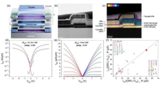
The development faced two primary technical hurdles: balancing the inherently mismatched driving capabilities of P-type and N-type carbon nanotube transistors, and preventing high-temperature fabrication steps from degrading the performance of underlying device layers. To resolve these issues, the research team introduced a novel doping-free CMOS design strategy that optimizes transistor geometry to ensure matched electrical characteristics while thermally insulating lower layers during upper-layer processing. This innovative structural approach enabled the successful fabrication of highly stable all-carbon nanotube CFET inverters that operate reliably across a broad voltage range of 0.2 V to 1 V with low power consumption. At just 1 V, the devices achieved a peak voltage gain of 164, setting a new record for low-dimensional semiconductor CFETs and confirming their suitability for complex digital logic operations.
Building on these high-performance components, the team successfully integrated them into complete digital circuits, including basic AND, OR, NAND, and NOR gates, as well as a four-transistor static random-access memory (SRAM) cell. Most notably, they constructed the world’s first five-stage ring oscillator using this all-carbon nanotube CFET architecture, marking a decisive step from single-device validation to system-level implementation. This milestone not only demonstrates the practical viability of carbon nanotube-based vertical stacking but also establishes a foundational blueprint for next-generation high-density, low-power integrated circuits that could ultimately overcome the limitations of traditional silicon technology.
The development faced two primary technical hurdles: balancing the inherently mismatched driving capabilities of P-type and N-type carbon nanotube transistors, and preventing high-temperature fabrication steps from degrading the performance of underlying device layers. To resolve these issues, the research team introduced a novel doping-free CMOS design strategy that optimizes transistor geometry to ensure matched electrical characteristics while thermally insulating lower layers during upper-layer processing. This innovative structural approach enabled the successful fabrication of highly stable all-carbon nanotube CFET inverters that operate reliably across a broad voltage range of 0.2 V to 1 V with low power consumption. At just 1 V, the devices achieved a peak voltage gain of 164, setting a new record for low-dimensional semiconductor CFETs and confirming their suitability for complex digital logic operations.
Building on these high-performance components, the team successfully integrated them into complete digital circuits, including basic AND, OR, NAND, and NOR gates, as well as a four-transistor static random-access memory (SRAM) cell. Most notably, they constructed the world’s first five-stage ring oscillator using this all-carbon nanotube CFET architecture, marking a decisive step from single-device validation to system-level implementation. This milestone not only demonstrates the practical viability of carbon nanotube-based vertical stacking but also establishes a foundational blueprint for next-generation high-density, low-power integrated circuits that could ultimately overcome the limitations of traditional silicon technology.