Chinese semiconductor thread II

tokenanalyst

Lieutenant General
Registered Member

The National Innovation Center for Information Optoelectronics has successfully developed a 250GHz ultra-wideband photonic chip.​

The National Innovation Center for Optoelectronics (NOEIC) recently successfully developed an ultra-wideband photonic chip. Despite being less than 1 cm long and 1 mm wide, this chip boasts a record-breaking 250 GHz bandwidth, setting a new world record for similar devices and providing new underlying hardware support for the development of optical communication and 6G technology.

In fiber optic communication networks, photonic chips act like "translators" and "postmen" in the physical world. Our everyday devices, such as mobile phones and computers, process electrical signals, while data needs to be converted into optical signals to reduce loss and increase speed during long-distance transmission. Photonic chips are the key components responsible for the "electro-to-optical" and "optical-to-electrical" conversions. The larger the chip's bandwidth, the more data it can carry and transmit per unit of time.
1778859649224.png

Based on this ultra-wideband photonic chip, the project team successfully achieved cross-network integration of optical fiber communication and wireless communication systems, reaching a world-leading level in transmission rate.

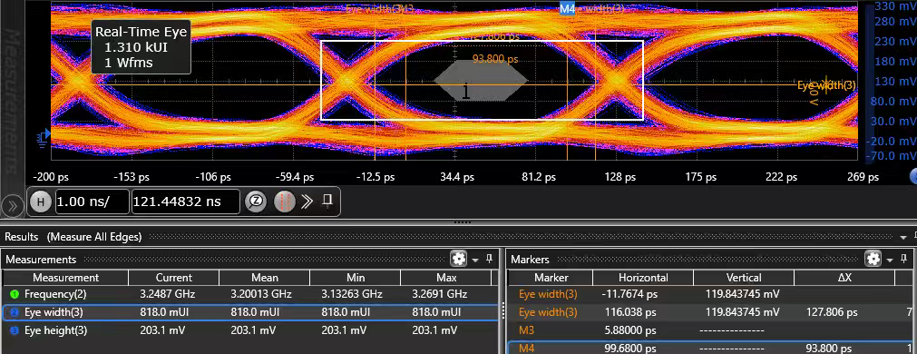
Official data shows that the single-channel speed of fiber optic wired transmission exceeds 512Gbps, which is equivalent to downloading more than a dozen high-definition movies in one second; the single-channel speed of terahertz wireless transmission reaches 400Gbps, which is enough to provide 8K ultra-high-definition video streams for 86 users at the same time.

Zhang Hongguang, manager of the Future Technology Department at the center, explained that based on the underlying technology of this chip, the R&D team has developed the world's first 170 GHz intensity modulator, which has been successfully applied to domestically produced optoelectronic measurement equipment. In the future, this chip will serve as a core technology component, providing underlying support for 6G "space-air-ground integrated" communication networks, and is expected to be extended to spaceborne communication equipment, further contributing to the development of domestically produced satellite communication.​

Please, Log in or Register to view URLs content!
 

tokenanalyst

Lieutenant General
Registered Member

Niu Core's domestically developed advanced DDR5/LPDDR5 IP both break through 6400Mbps​


With the rapid development of large-scale artificial intelligence models and autonomous driving, the amount of data is growing rapidly, and the demand for data throughput capacity in systems continues to rise. Many computing chips, despite possessing extremely high theoretical computing power, often struggle to fully realize their actual performance due to limited data transmission bandwidth. This bottleneck of mismatch between storage and computing speed makes high-speed storage interface IP a key battleground for unlocking the actual performance of chips.

NiuXin Semiconductor has successfully verified high-performance DDR5/LPDDR5 IPs at 6400Mbps using domestically developed advanced processes. Notably, while NiuXin had previously achieved a measured DDR5 IP speed of up to 8400Mbps on more advanced process nodes, this achievement on domestically developed advanced processes still pushes the speed to 6400Mbps, fully demonstrating the company's core strength in bridging the generational gap through architectural and circuit design innovation. Leveraging its combined advantages of "high performance + low cost + supply chain security," NiuXin provides customers with a new differentiated path.​

In terms of core specifications, BullChip's DDR5 IP achieves a stable speed of 6400Mbps using advanced domestic manufacturing processes and supports the latest DFI 5.1 interface specification. Its LPDDR5 IP also reaches 6400Mbps, with a system bandwidth of 51.2GB/s at a 64-bit bus width. Compared to the specifications of products from major international manufacturers at the same process node, BullChip achieves comparable or superior performance in key dimensions such as data rate, interface version, and frequency switching flexibility.

1010157191272.0066.png


LPDDR5 6400Mbps eye diagram

Breakthroughs in ecosystem compatibility are equally significant. This IP solution is fully compatible with domestically produced DDR5/LPDDR5 memory chips, truly establishing a fully domestic supply chain from interface IP to physical chips, and from design tools to manufacturing processes. This means that customers can complete complete system design verification and mass production without relying on memory chips from specific overseas brands, significantly improving the self-control of the supply chain.

Currently, several key partners of NiuChip have achieved significant milestones in project verification. This IP solution demonstrates outstanding environmental robustness, supporting a junction temperature range of -40℃ to 125℃ and ESD protection up to 2000V using a human body model. It can meet the stringent environmental requirements of various scenarios, from data center air-cooled cabinets to high-temperature automotive enclosures. Whether operating under continuous high temperatures inside a server chassis or experiencing severe temperature fluctuations near a car engine compartment, this IP maintains stable signal quality and bit error rate performance.

Please, Log in or Register to view URLs content!
kniulink.com/index/index/product?sid=2​
 

tokenanalyst

Lieutenant General
Registered Member

Huahai Qingke's Master-BN300 edge polishing equipment has secured repeat orders from a leading domestic chip manufacturer.​


Recently, Huahai Qingke Co., Ltd. (hereinafter referred to as "Huahai Qingke" successfully secured repeat orders from leading domestic chip companies for its independently developed 12-inch wafer edge polishing equipment, Master-BN300. This not only signifies that the performance of this machine has won high recognition and deep trust from leading customers, but also demonstrates Huahai Qingke's strong equipment support for high-quality development in fields such as memory chips and advanced packaging amidst the wave of Al-driven structural transformation in the semiconductor industry.​

1778862182376.png

With the rapid development of AI-related applications, storage technologies such as HBM (High Bandwidth Memory) and 3D NAND have become key pathways to improve chip performance. These technologies often employ multi-layer stacking and heterogeneous integration processes, placing higher demands on the precision control of wafer manufacturing.

Huahai Qingke's Master-BN300 edge polishing equipment integrates three core functional modules: high-precision polishing, efficient cleaning, and accurate measurement. It effectively solves process challenges such as burrs and uneven morphology at wafer edges. While improving the precision and inter-wafer repeatability of edge polishing, this equipment significantly reduces the risk of edge defects in subsequent wafer manufacturing processes, thereby greatly improving chip mass production yield. Currently, the overall performance of this equipment has reached international advanced levels.


This repeat order for the Master-BN300 is another significant achievement for Huahai Qingke in deepening its "equipment + service" platform development strategy. While maintaining a leading domestic market share in CMP equipment, the company is gradually expanding its product line to cover more key aspects of integrated circuit manufacturing, forming a diversified business layout encompassing CMP equipment, ion implantation equipment, thinning equipment, scribing equipment, edge polishing equipment, wet processing equipment, wafer regeneration, and consumable maintenance services. In the future, Huahai Qingke will continue to adopt a forward-looking global perspective, building an even richer product matrix to provide customers with more advanced semiconductor high-end equipment and complete solutions, contributing to industrial upgrading and high-quality development.​

Please, Log in or Register to view URLs content!
 

tokenanalyst

Lieutenant General
Registered Member

Huahai Qingke's first 8-chamber 12-inch cleaning machine officially rolled off the production line.​


Huahai Qingke's first 8-chamber 12-inch single-wafer cleaning machine for the large silicon wafer manufacturing field was successfully delivered and officially sent to a leading domestic large silicon wafer company, marking another hard-core product in the domestic wet cleaning equipment industry.

The 8-chamber 12-inch single-wafer cleaning machine shipped this time is a key achievement of Huahai Qingke in its deep cultivation of semiconductor wet process equipment. The equipment adopts a stacked architecture, which is adapted to the precision manufacturing needs of 12-inch large-size silicon wafers. It can provide downstream customers with high-quality, high-stability wafer cleaning equipment and overall solutions, effectively meeting the stringent process standards of large silicon wafer production and making up for the shortcomings of domestic large silicon wafer manufacturing equipment.

Semiconductor cleaning is a core process in wafer manufacturing, directly impacting chip yield and performance. 12-inch silicon wafers are the fundamental carrier for advanced process chips. Currently, China's large silicon wafer industry is accelerating its localization process, leading to a continuous increase in demand for high-end wet cleaning equipment. For a long time, core equipment in this field has been highly dependent on overseas manufacturers. The launch of Huahai Qingke's new product will effectively break the monopoly of foreign equipment and increase the penetration rate of domestically produced equipment in the large silicon wafer market.

As a leading domestic semiconductor equipment manufacturer, Huahai Qingke continues to expand its presence in core equipment sectors such as chemical mechanical polishing (CMP) and wet cleaning, constantly improving its high-end semiconductor equipment product portfolio. The successful delivery of this 8-chamber 12-inch single-wafer cleaning machine further validates the company's technological R&D capabilities in the field of wet process equipment and solidifies its leading position in the domestic semiconductor equipment market.

Please, Log in or Register to view URLs content!
 

tokenanalyst

Lieutenant General
Registered Member

Jingsheng 300 mm SiC pilot line progress.​

Jingsheng Mechanical & Electrical disclosed the latest progress: its order backlog exceeds 3.7 billion yuan, and the 12-inch silicon carbide pilot line has completed sample delivery.​

  • Strong Order Backlog: As of the end of 2025, the company's outstanding contracts for integrated circuit and compound semiconductor equipment exceeded RMB 3.7 billion, representing a 12% increase year-over-year. This includes approximately RMB 3 billion in large silicon wafer orders, which now serve as the primary revenue driver.​
  • Silicon Carbide (SiC) Breakthroughs: Jingsheng Mechanical & Electrical stated that its 6-8 inch silicon carbide substrates have achieved mass production and sales, with the yield of 8-inch products remaining stable at around 75%, and core parameters reaching advanced industry levels. The company has secured bulk orders from numerous domestic and international customers, with products primarily targeting applications such as 800V high-voltage platforms for new energy vehicles. Relevant customers include Tesla , Infineon , BYD , and StarPower Semiconductor .​
  • 12-Inch Pilot Line: A major milestone was reached with the completion of sample verification on its 12-inch SiC pilot line. The 12-inch silicon carbide substrate processing pilot line has been officially put into operation and has completed sample verification. The company stated that it has overcome key technical challenges such as uneven temperature field during crystal growth and crystal cracking, achieving independent R&D across the entire process from crystal growth and processing to testing equipment.
1778862813470.png

Strategic Expansion & Innovation

  • Product Diversification: Beyond wafers, Jingsheng is expanding into advanced packaging and key equipment fields like depressurized epitaxy and Atomic Layer Deposition (ALD) thin film deposition to support domestic substitution in the chip industry.​
  • R&D Commitment: The company maintains high innovation levels with 2025 R&D investments of RMB 955 million (8.41% of revenue), a portfolio of 1,274 valid patents, and an R&D team where over 38% hold master's degrees or higher.​
Please, Log in or Register to view URLs content!
 

tokenanalyst

Lieutenant General
Registered Member

Zhongke Feice's Semicon SEA 2026 event concluded successfully, showcasing its comprehensive industry chain capabilities to support overseas expansion.​


Throughout the three-day exhibition, the Zhongke Feice team maintained high enthusiasm, engaging in sincere and in-depth exchanges with every visitor. Behind this focus lies Zhongke Feice's absolute confidence in its product coverage and technological depth.

Currently, the company's products and customer base cover the entire semiconductor industry chain-from substrate manufacturing and front-end chip manufacturing to advanced packaging, from silicon-based semiconductors to third-generation semiconductors, CAS Test's presence is ubiquitous. The company's metrology and inspection equipment has been operating stably for a long time in thousands of processes at leading domestic wafer foundries, continuously verifying its unparalleled reliability. This ultimate trust honed on the production line is forging the strongest protective armor for the company's overseas expansion.

The new product from the dual stars in the light and dark fields breaks the deadlock.
Addressing customers' pain points regarding yield rates

At this exhibition, the company launched two major new product series: the SYCAMOREDFI dark field nanopatterned wafer defect inspection series and the REDWOODBBP bright field nanopatterned wafer defect inspection equipment. These two product series precisely address core pain points in the industry, providing higher defect detection rates at smaller process nodes and accurately helping customers achieve breakthroughs in yield and quality.
Currently, the dark field nanopatterned wafer defect inspection equipment has been verified and mass-produced by several leading logic and memory customers in China, while the bright field nanopatterned wafer defect inspection equipment is steadily progressing towards production line verification by several leading domestic customers.
1778868654383.png1778868695201.png
This impressive debut at SEMICON SEA marks a significant step forward for CAS Test & Measurement in the Southeast Asian market. CAS Test & Measurement stated that it will continue to expand its business in Southeast Asia and steadfastly use it as a strategic foundation to systematically extend its reliable end-to-end yield management solutions to the global semiconductor industry. The company hopes that its superior metrology equipment and intelligent software from China will become a key engine for improving global semiconductor yields.​

Please, Log in or Register to view URLs content!
 

tokenanalyst

Lieutenant General
Registered Member

New Wear Model Extends Echelle Grating Tool Life​


Researchers from China's Changchun Institute of Optics, Fine Mechanics and Physics (CIOMP) have developed an innovative wear threshold model designed to extend the life and enhance the precision of diamond ruling tools used for manufacturing echelle gratings. As these high-resolution optical components are critical for advanced applications ranging from astronomy and semiconductor inspection to biomedical sensing, even minor geometric errors caused by gradual tool wear can severely compromise their diffraction efficiency. This research, published in the Journal of Manufacturing Processes, addresses these challenges by shifting the focus of quality assessment from traditional mechanical parameters to direct measurements of grating optical performance.

To achieve this breakthrough, the study employed Rigorous Coupled-Wave Analysis (RCWA) to model how changes in tool condition affect groove shape and subsequent light diffraction. The resulting quantitative mapping identifies a specific "wear threshold" beyond which grating quality deteriorates rapidly; prior to this point, performance remains stable despite minor degradation. This insight empowers manufacturers to accurately predict when tools require re-sharpening, thereby preventing production failures, reducing waste, and optimizing fabrication time in high-stakes environments like space observation and precision spectroscopy.

The model was validated through extensive experiments on CIOMP's ultra-precision ruling platform, where fabricated gratings closely matched theoretical predictions across various tool geometries. Notably, the research found that designs featuring smaller groove bottom angles exhibit greater wear tolerance, maintaining stable performance over longer manufacturing distances. By transforming tool wear assessment from a purely mechanical issue into an optical performance criterion, this work offers a practical, scalable framework for the reliable production of next-generation diffraction gratings essential to advanced manufacturing fields that depend on large-area, high-efficiency gratings, including space observation, semiconductor lithography, and precision spectroscopy

Please, Log in or Register to view URLs content!


tokenanalyst

Lieutenant General
Registered Member

Driver wavelength and intensity dependence of extreme ultraviolet emission from laser-produced tin microdroplet plasmas​


Abstract​

Extreme ultraviolet (EUV) lithography sources driven by laser-produced tin (Sn) plasmas require optimal matching of driver laser parameters to maximize in-band conversion efficiency (CE) and spectral purity (SP). In this work, we systematically investigate the driver wavelength (1.064–10.6 µm) and intensity dependence of EUV emission from Sn microdroplets using the two-dimensional radiation-hydrodynamics code RHDLPP and its three-dimensional spectral post-processing module SpeIma3D. Our simulations reveal a fundamental physical trade-off governing source performance. Short-wavelength drivers (e.g., 1.064 µm) efficiently couple energy into dense plasma regions but suffer from severe in-band radiation trapping and opacity broadening, limiting maximum CE and SP. Conversely, long-wavelength drivers (e.g., 10.6 µm) produce highly transparent coronas that yield excellent SP (up to ∼29.4%) but suffer from significantly reduced absolute emission measures, thereby capping the overall CE. By mapping the wavelength-resolved escape factor and spatial emission distributions, we identify the mid-infrared range (4.0–5.0 µm) as an optimal operating window. In this regime, a favorable balance between sufficient intrinsic emissivity and mitigated optical depth is achieved, yielding a maximum predicted CE of ∼3.41%. These findings provide a comprehensive physical scaling and valuable guidelines for the development of alternative mid-infrared solid-state laser drivers for next-generation EUV lithography sources.

1778870873954.png

Please, Log in or Register to view URLs content!
 

huemens

Junior Member
Registered Member
Trump was asked about if H200 came up in discussions. Here's his response. First he said it didn't come up, then he said it did come up.
Q: Chips like the H200s that Jensen has. Did that come up at all with him?
A:
It didn't come up, but as you know Jensen was there. He's a amazing guy at Nvidia. And he would be in... You know, they have much higher level than the H200, but the H200 is good. Uh, China needs it. And so yeah it came up. They haven't bought any so much, you know. Because they chose not to. They wanna try and develop their own. But it did come up and I think something could happen on that.
 
Top