Chinese semiconductor thread II

tokenanalyst

Lieutenant General
Registered Member

Kaixin Institute adopted GalaxSim, a high-performance digital emulator from Chipone Technology, and achieved nearly 3 times efficiency improvement in RISC-V verification.​


Xinhuazhang Technology (a system-level verification EDA provider) and the Beijing Open Source Chip Research Institute (OpenCore) successfully deployed GalaxSim Turbo 3.0, a high-performance digital emulator from Xinhuazhang, to significantly improve the verification efficiency of the "Xiangshan" third-generation Kunming Lake RISC-V processor—achieving nearly a threefold increase in verification speed.
1763131913428.png
  • Dual-engine simulation (event-driven and cycle-driven) enables faster, more accurate verification without altering existing test environments.​
  • GalaxSim Turbo 3.0 addresses major bottlenecks in open-source chip development—including long verification cycles and complex debugging—by offering:
    • Full support for SystemVerilog and UVM with advanced features like SVA and Functional Coverage​
    • One-click switching between test cases​
    • Seamless integration into existing verification flows, reducing maintenance costs​
    • Dynamic thread management (runtime vs. compile-time), improving parallel efficiency​
    • Intelligent resource allocation and optimized performance based on design characteristics​
    • Enhanced debugging via XEDB waveform merging and coverage analysis​
Tang Dan, Dean of the Open Source Institute, emphasized that GalaxSim’s capabilities have enabled faster iteration while maintaining accuracy—crucial for architectural innovation—and significantly reduced R&D costs. The decision to free GalaxSim for use by the institute boosts access to high-quality domestic EDA tools, accelerating chip development in AI and HPC.

Xie Zhonghui, co-CEO of Xinhuazhang, noted that this success stems from real-world validation through the "Xiangshan" benchmark project. By making GalaxSim freely available, the company aims to:
  • Lower entry barriers for startups​
  • Shorten product development cycles​
  • Strengthen collaboration between EDA and chip industries​
  • Foster independent innovation in China’s domestic RISC-V ecosystem​
This partnership marks a milestone in advancing China's open-source semiconductor industry by enabling more teams to leverage production-grade, scalable verification tools—accelerating progress toward self-reliance in high-performance computing and AI chips.

Please, Log in or Register to view URLs content!
 

tokenanalyst

Lieutenant General
Registered Member

Photoresist company Qigong Zhiyuan lands in Lingang, Shanghai​


On the morning of November 6, Shanghai Qigong Zhiyuan Technology Co., Ltd. (hereinafter referred to as "Qigong Zhiyuan") officially moved into the Shanghai Lingang Blue Bay Future Industry Innovation Center.

Qigong Zhiyuan is an innovative company specializing in semiconductor photoresists and related materials. It was jointly founded and invested in by Shanghai Junhua Fuchuang Electronic Materials Industry Development Private Equity Fund and others. The company is committed to developing high-performance, high-reliability electronic materials to meet the needs of high-end manufacturing fields such as semiconductors and integrated circuits. With its innovative technology and R&D capabilities, Qigong Zhiyuan demonstrates strong competitiveness in the industry. In October 2025, Qigong Zhiyuan received exclusive angel round investment from Guotai Junan Innovation Investment.

Photoresist is a core material in semiconductor manufacturing. It has high technological barriers and an urgent need for domestic production. It is a "key link" in achieving self-reliance and control of the industrial supply chain.

According to Lingang Lanwan, Qigong Zhiyuan, leveraging its deep technological accumulation, has vertically integrated the entire industrial chain from monomer to resin synthesis to blending, and continues to exert its strength in product development, supply chain localization, and mass production technology. The company's products have successfully completed certification at major FAB manufacturers in China and have achieved rapid monthly sales growth, demonstrating strong technological capabilities and market potential.

Please, Log in or Register to view URLs content!
 

tokenanalyst

Lieutenant General
Registered Member

Highly efficient "self-exfoliation"! Ningbo Institute of Materials Technology and Engineering achieves rapid fabrication of 4-inch diamond "self-supporting" ultrathin films.​


the research team at the Ningbo Institute of Materials Technology and Engineering, Chinese Academy of Sciences, successfully prepared a 4-inch self-supporting diamond ultrathin film with ultra-low warpage, marking an important step towards bonding diamond thin films to chips.

1763132488586.png

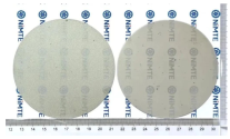
Recently, the team has achieved another breakthrough in the efficient exfoliation technology of diamond ultrathin films, establishing a "self-exfoliation" technology for 4-inch ultra-low warp diamond ultrathin films. Through precise control and process innovation of the initial nucleation and growth of diamond films, the synthesized 4-inch diamond film (thickness <100μm), after grooving, can achieve perfect and damage-free separation from the Si substrate solely by its own gravity, without any external force assistance, thus preparing a flat "self-supporting" ultrathin film (Figure 1, video). This technology reduces the exfoliation time from several hours required by etching to just a few minutes, not only reducing costs and increasing speed, but also overcoming the environmental hazards of chemical etching, opening up an innovative path for the efficient and green manufacturing of high thermal conductivity, self-supporting diamond ultrathin films.
1763132508436.png
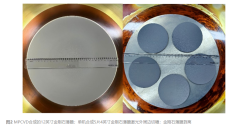
Furthermore, with the support of a major equipment project from the Chinese Academy of Sciences, the team successfully expanded the diamond deposition area of 915MHz high-power MPCVD to 12 inches, achieving simultaneous synthesis of five 4-inch diamond films with low stress and ultra-low warpage in a single machine (Figure 2). Combined with the aforementioned efficient "self-peeling" technology, this lays a solid foundation for the equipment and process of industrial-scale mass production of such "self-supporting" diamond films.

1763132547190.png

Please, Log in or Register to view URLs content!
 

tokenanalyst

Lieutenant General
Registered Member

TCL CSOT Printing Achieves Breakthrough in Small-Size OLEDs, Encompassing Technological Innovation Across the Entire Industry​


At DTC2025 (TCL CSOT Global Display Ecosystem Conference) in Suzhou, TCL CSOT unveiled major breakthroughs in display technology, particularly in small-size printed OLED, while advancing AI integration and visual health innovation.​
  • AI Integration: Introduced Star Intelligence X-Intelligence 3.0, the first large-scale AI model in the display industry with strong inference capabilities. Built on a "Five-Star AI Architecture" (1 Lake, 1 Model, 3 Platforms), it enhances R&D, manufacturing, and operations through data-driven optimization improving yield, scheduling, and virtual simulation.
  • Printed OLED Breakthroughs:
    • Launched the world’s first Real Stripe RGB OLED mobile phone display (5.65") with a resolution of 390 PPI and visual sharpness equivalent to 490 PPI.​
    • Demonstrated green manufacturing benefits: printed OLED reduces energy use by up to 300–400 million kWh annually enough to power a 500,000-person city for 30–60 days.​
    • Showcased high-resolution displays (e.g., 2.56 PPI glass-based OLED, 0.28" silicon micro-LED), proving leadership in full-display technology.​
  • Visual Health Focus: Released the Visual Health White Paper 2.0, based on research into natural light characteristics (broad spectrum, non-polarized, continuous, etc.). TCL CSOT’s displays now closely mimic natural light through technologies like XRGB and global DC (1 nit), reducing eye strain. Collaborated with National Eye Center, Lenovo, TAL Education Group, and CVTE to develop child-friendly educational screens featuring "one screen, three modes," diffused layers, and a 7:5 golden ratio for better focus and well-being.​
  • Sustainability & Ecosystem Vision: Emphasized green development ("two lows and one high" in manufacturing) and positioned printed OLED as part of an independent, sustainable display ecosystem. The brand APEX sets industry standards across four pillars: Picture Quality, Visual Health, Green Sustainability, Future Imagination.​
  • Leadership & Collaboration: Under CEO Zhao Jun’s vision, TCL CSOT is driving a two-way innovation loop “AI for Display” and “Display for AI”to create interactive, human-centered screens. The company aims to shift from technology leadership to ecosystem leadership, collaborating globally to advance the display industry.​
TCL CSOT reaffirms its role as a global leader in next-generation displays, combining cutting-edge innovation with sustainability and user-centric design.

Please, Log in or Register to view URLs content!
 

tokenanalyst

Lieutenant General
Registered Member

Jiaocheng Ultrasonic: Orders for wafer-level ultrasonic scanning microscopes have been received and deliveries are underway.​


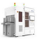
Recently, during an institutional survey, Jiaocheng Ultrasonic stated that its independently developed wafer-level ultrasonic scanning microscope is mainly used in the semiconductor packaging and testing process. It can perform non-destructive testing on defects in semiconductor wafers, 2.5D/3D packaging, panel-level packaging, and other products. Currently, the product has secured orders from well-known domestic customers and is being delivered successively.

1763133142573.png

In this field, companies such as Germany's PVA and the US's Sonoscan hold the majority of the market share. Jiaocheng Ultrasonic believes that with further enhancements in its ultrasonic equipment technology, continuous optimization of equipment specifications, and further improvements in performance parameters, its wafer-level ultrasonic scanning microscope is expected to unlock greater value in the semiconductor packaging and testing field, opening up a broader market space.

According to reports, in the power semiconductor field, Jiaocheng Ultrasonic offers a full range of ultrasonic solutions, including ultrasonic terminal welding machines, ultrasonic PIN welding machines, ultrasonic bonding machines, and ultrasonic scanning microscopes, all of which are already in mass production. In this field, the company maintains strong partnerships with well-known enterprises such as SAIC Infineon, CRRC Times Electric, Zhenhua Technology, Hongwei Technology, Silan Microelectronics, Xinlian Integrated Circuits, and CR Microelectronics.

In the field of advanced semiconductor packaging, JAO Cheng Ultrasonic is vigorously promoting the research and development and promotion of new products and equipment such as advanced ultrasonic scanning microscopes and ultrasonic die bonders (ultrasonic thermoforming machines). The company's advanced packaging-related businesses are continuously breaking through the boundaries of technology and market, and accelerating towards large-scale application.

Please, Log in or Register to view URLs content!
 

tokenanalyst

Lieutenant General
Registered Member

Southchip Technology launches millimeter-wave radar PMIC to build a complete integrated sensing solution.​


Southchip Technology launched the SC6207Q, an ASIL-B compliant millimeter-wave radar PMIC designed for automotive applications. The single-chip solution offers high efficiency (>80%), multi-channel voltage outputs (including 2.5V–5V buck converters, dual low-voltage channels, and a boost converter), and excellent noise suppression, enabling stable radar performance in adverse weather and low-light conditions.

1763133383055.png
With its compact 5mm×5mm QFN-28 package, the SC6207Q simplifies PCB design and improves system integration. Its high efficiency reduces thermal noise and voltage fluctuations, enhancing imaging accuracy and consistency. Operating at a fixed 2.1MHz PWM frequency with programmable spread spectrum modulation, it minimizes electromagnetic interference and requires fewer external components.

The PMIC meets strict automotive safety standards through integrated diagnostics (BIST, watchdog timer), redundancy circuits, temperature/load compensation (±1% error), and protection features like over-temperature and short-circuit safeguards.

By combining the SC6207Q with its camera PMICs (SC6201Q/05Q), Southchip offers a complete, reliable fusion sensing solution for ADAS systems. With millimeter-wave radar installation reaching 57.3% in China’s passenger vehicles by July 2024 6.53 million units, the market potential is growing rapidly.

This launch marks Southchip’s expansion of its automotive-grade PMIC product line, supporting intelligent driving and fusion perception across cameras, radar, and other key subsystems.


Please, Log in or Register to view URLs content!
 

tokenanalyst

Lieutenant General
Registered Member

A First-Principles Scaling Law for the Recoil Velocity of Laser-Irradiated Tin Microdroplets: A Theoretical, Experimental, and Numerical Validation​

Abstract​

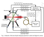
Precise control over the recoil dynamics of laser-irradiated tin microdroplets is paramount for the efficiency of extreme ultraviolet (EUV) light sources, the core of modern semiconductor manufacturing. However, predictive models have hitherto been purely empirical, lacking a physical foundation and thus limiting the optimization of next-generation laser strategies. We resolve this by establishing and rigorously validating a universal scaling law derived from the first principles of momentum conservation. Through an integrated theoretical, experimental, and numerical approach, the law is validated across three orders of magnitude in laser energy (0.01–60 mJ). It demonstrates near-perfect agreement with experimental data (coefficient of determination R2 = 0.998) and accurately predicts the measured ablation threshold. This work distills the complex multiphysics of laser-droplet interaction into an elegant and predictive framework, establishing a fundamental benchmark for optimizing advanced multi-pulse schemes. Ultimately, it provides the theoretical cornerstone for precisely modulating plasma properties and mitigating debris, unlocking new pathways to enhance the overall performance of EUV sources.

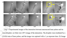
1763133883564.png1763134046747.png

Please, Log in or Register to view URLs content!
 

tokenanalyst

Lieutenant General
Registered Member

Moore Threads to launch IPO on November 24, to rise 8 billion yuan to further invest in high-end GPUs.​


Moore Threads, a Chinese AI and high-performance computing company founded in 2020, will launch its IPO on November 24 on the Science and Technology Innovation Board (STAR Market) with stock code 688795 and online subscription code 787795. The offering involves 70 million shares, representing 14.89% of post-offering share capital, and aims to raise 8 billion yuan.

The funds will be used for R&D in next-generation AI training, graphics, and AISoC chips, as well as working capital expansion focusing on achieving independent control over high-end GPU technology.

Moore Threads has developed its proprietary MUSA converged GPU architecture, supporting AI computing, graphics rendering, physics simulation, and scientific computing on a single chip. This innovation enables flexibility, scalability, and compatibility with global ecosystems, reducing developer migration costs.

Financially, the company has shown strong growth: revenue rose from 46 million yuan in 2022 to 438 million yuan in 2024, with AI products driving 94.85% of first-half 2025 revenues (665 million yuan). Key products like "Quyuan" and "Pinghu" have achieved significant sales, and the company has secured over 2 billion yuan in orders, with more than 1.7 billion yuan from AI projects.

Despite still being behind international giants in R&D depth, Moore Threads is seen as a key player in advancing China’s independent semiconductor capabilities, particularly in GPUs critical for AI, big data, and cloud computing. The IPO supports national strategies to promote technological self-reliance and build new computing infrastructure.

Moore Threads expects to become profitable by 2027 and aims to expand its presence across enterprise, government, data center, and consumer markets through integrated cloud-edge-device solutions. Its listing marks a major milestone for China’s domestic GPU innovation and the broader high-end chip industry.​

Please, Log in or Register to view URLs content!
 

tokenanalyst

Lieutenant General
Registered Member

Mask defects characterization techniques based on synchrotron radiation extreme ultraviolet light source​

Abstract​

The multilayer structure of extreme ultraviolet (EUV) masks limits the penetration depth of traditional inspection techniques at non-working wavelengths, thus hindering the effective examination of buried phase defects. Developing defect characterization techniques operating at the 13.5 nm wavelength is crucial for overcoming the quality bottleneck in EUV mask fabrication. Synchrotron radiation light source, with their stable EUV wavelength, cleanliness, and high power density, represents an ideal light source for EUV mask defect characterization research. In this work the current state of technology development for mask characterization at the world's four major synchrotron radiation facilities are systematically reviewed. Through comparative analysis, their working principles, technical advantages, and limitations are investigated in depth, and provide a forward-looking discussion on future trends. In response to the specific requirements for EUV mask defect detection and review, this paper discusses the requirements for the next-generation system platform, which integrates deep detection and review functions, develops novel compact light sources, and innovatively combines the advantages of various imaging techniques to improve the numerical aperture ( NA ) of imaging systems. This aims to achieve a theoretical resolution of over 20 nm, meeting the future demands of the EUV lithography industry for higher NA (>0.55) and shorter wavelengths (6.7 nm). Regarding the prospects of extending synchrotron radiation to industrial applications, a compact synchrotron radiation source, which can be developed on-site in semiconductor facilities, is introduced to accelerate the research and development cycle, while achieving the synergistic integration of imaging technologies. This paper focuses on the application of phase recovery principle of ptychography to Fourier synthesis illumination (FSI), achieving aberration correction in lens-based systems through synthetic aperture extension. In this paper, the working principles, performance benchmarks, technical challenges, and emerging development trends of existing synchrotron radiation-based EUV mask characterization techniques are investigated. It provides an important reference for designing next-generation EUV mask characterization system platforms.
1763136934136.png

SSRF-BL09B1A​

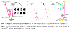
SSRF built an integrated system platform for online detection and analysis of EUV mask defects, SSRF-BL09B1A, on the BL09B beamline, covering an energy range of 80-500 eV. Its configuration includes two grating monochromators with line densities of 50 l/mm and 250 l/mm, which can achieve energy resolutions E /ΔE ( 92 eV) of approximately 1000 and 8000 respectively [ 2 , 3 ] to meet the imaging requirements of zone plates with different NAs . As shown in Figure 2(c), the optical path design of SSRF-BL09B1A is similar to that of SHARP, that is, it uses the same three-mirror FSI system, and can also focus the EUV beam onto the mask surface by 10 times. Unlike SHARP, SSRF-BL09B1A additionally uses an SCMOS detector to directly collect the dark field signal of the mask reflected light, and can use dark field spatial correlation spectrum technology to quickly find and locate the suspected defect location, and realize the online detection function [ 27 ] . When the defect-free area of the mask is exposed, SCMOS only acquires zero-order light, i.e., the bright field signal; when a defect is exposed, SCMOS also acquires weak diffraction signals outside the zero-order light region, i.e., the dark field signal. Since the defect size is in the tens of nanometers, the dark field signal is very weak compared to the millimeter-sized light spot at the mask. Therefore, to improve sensitivity, spatial correlation calculations need to be performed on the nearby dark field signals. When a defect appears, observing the abrupt change in the correlation spectral function value can quickly identify the suspected location of the defect.

The analysis section of SSRF-BL09B1A still uses off-axis zone plates to amplify the mask reflected light to CCD for full-field imaging. Based on the three-mirror FSI system to form a large NA angle, the illumination conditions with arbitrary filling patterns can be achieved through programming , as shown in Figure 2(a). At the same time, by configuring off-axis zone plates with different NAs , the analysis of the located defects can achieve a theoretical resolution of better than 20 nm [ 27 ] . To date, for a 6-inch EUV mask, the defect analysis resolution of SSRF-BL09B1A using an off-axis zone plate with 4× NA = 0.5 and single coherent illumination has reached 48 nm hp. In the future, an off-axis zone plate with 4× NA = 0.625 and FSI will be used for further optimization.

Compact Accelerator Light Source​

Although synchrotron radiation EUV light sources have advantages such as stable wavelength, cleanliness and pollution-free operation, and tunable wavelength, their facility dependence and time cost are still bottlenecks for industrial applications. Therefore, compact accelerator light sources with small size have attracted the interest of some international research institutions and commercial institutions. For example, the PAL-EUV device built by the Pohang Accelerator Laboratory (PAL) in South Korea in 2022 has generated EUV light with a beam energy of 400 MeV in size of only 11.5 m × 11.5 m [ 5 ] . However, the external facilities of PAL-EUV are too large, with a main ring circumference of about 40 m and an area of more than 130 m2 [ 5 ] , which is not conducive to industrial applications.

PSI proposed a compact low-emissivity accelerator design, namely the compact storage ring for actinic mask inspection (COSAMI) [ 6 ] . To resolve the conflict between compactness and low emissivity and to maintain high beam brightness, COSAMI uses a third-generation diffraction-limited storage ring. Through the so-called "top injection" technique, the storage ring is superimposed on an intensifier at a higher position, while the linear accelerator injector is installed within the perimeter of the intensifier ring. The highly integrated design allows COSAMI to theoretically generate an electron beam energy of 430 MeV and an EUV beam with a flux of 1.35 × 10¹⁵ phs / s/0.1% BW while occupying an area of only 12 m × 5 m and a perimeter of only 25.8 m [ 6 ] . Unfortunately, this design has not yet been implemented, but the Chinese SSRF is also carrying out similar research and development work on a compact EUV accelerator light source, which is currently under construction.

Please, Log in or Register to view URLs content!
 

tphuang

General
Staff member
Super Moderator
VIP Professional
Registered Member
Please, Log in or Register to view URLs content!

Novosense's NovoGenius line of MCUs including MCUs for electric motor driver, ambient light driver and ultrasonic radar probe chip.
it's MCU+ product integrates MOSFT, LIN, in some cases PMIC, in other cases pre-driver
以纳芯微“MCU+”产品为例,NSUC1610集成了MOSFET、LIN总线,NSUC1800集成了电源IC,NSUC1602集成了预驱。
hard to go through the full article, but it does have a pretty wide scope of analog and logic chips, for EVs.

It has now achieved breakthrough in sales in Europe, Japan and Korea. for thermal management, it has entered supply chain for Global Tier 1 supplier.
 
Top