Chinese semiconductor industry

Status
Not open for further replies.

tphuang

Lieutenant General
Staff member
Super Moderator
VIP Professional
Registered Member
Please, Log in or Register to view URLs content!
Enkris semiconductor (晶湛半导体) is building China's largest production base of GaN power electronic materials, RF materials and microdisplay materials in Suzhou. Factory will be complete in Feb 2023. They will produce 120k 6 inch wafers and 120k 8 inch wafers a year. and then they will add another 10k of production a year it looks like?

In Dec 2021, they produced the world's first 12 inch, 1200V GaN wafer.

GaN is used prominently in military AESA radar, so there is potentially some usage here. But a whole, GaN seems like the next big thing after SiC.

On Nov 1, HG Semiconductor announced that it has started producing GaN power device wafer and will produce GaN power chips in start of 2024 after trial production in Q2 of 2023. GaN power chips have a lot of applications in new energy fields.
 

tphuang

Lieutenant General
Staff member
Super Moderator
VIP Professional
Registered Member
See, this is what I don't understand. Couldn't you just run more of these chips in parallel with some software optimization if you wanted to achieve the same performance as the A100. I couldn't tell from the article, but based on how quickly Nvidia throttled it, was it a software throttling of an A100 to downgrade to an A800? If so, whats stopping someone in China from basically "unlocking" it with the right skills?
I think that's why the entire thing is a joke. They could even just half the size of the chip to get under threshold also, but I guess reducing transmission speed is the easiest/cheapest way for them to nerf the performance to be under the threshold. Looks like Biren is doing the same. Eventually, I would assume they issue new orders to tighten certain criteria. But then the question is why don't they just make smaller chips that consume less power and stack more of them?

There is nothing preventing China from buying a whole bunch of V100 chips and stacking them together to get the same performance as A100. Sure, you might need more space and energy, but that's not a big issue for China. This is a country that builds exascale supercomputers with 14nm CPUs.

At some point (who knows how long), they might just say no AI chips at all that use any kind of American technology. By then, Chinese chip designers would've collaborated with SMIC already.
 

caudaceus

Senior Member
Registered Member
I think that's why the entire thing is a joke. They could even just half the size of the chip to get under threshold also, but I guess reducing transmission speed is the easiest/cheapest way for them to nerf the performance to be under the threshold. Looks like Biren is doing the same. Eventually, I would assume they issue new orders to tighten certain criteria. But then the question is why don't they just make smaller chips that consume less power and stack more of them?

There is nothing preventing China from buying a whole bunch of V100 chips and stacking them together to get the same performance as A100. Sure, you might need more space and energy, but that's not a big issue for China. This is a country that builds exascale supercomputers with 14nm CPUs.

At some point (who knows how long), they might just say no AI chips at all that use any kind of American technology. By then, Chinese chip designers would've collaborated with SMIC already.
Amdahl law is a thing.
i.e if you parallelize a system too much, it will spend all the time distributing, communicating and coordinating messages instead of working,
 

ansy1968

Brigadier
Registered Member
@tokenanalyst @hvpc @FairAndUnbiased @WTAN @BoraTas @latenlazy, what is a Particle Core Technology? What is their usage? and can it bypassed the need for an EUVL?

From the Video, it had stated China achievement and the futility of America led restriction.

1) the goal of made in China 2025 of achieving 70% domestic production are on track with mature technology up to 14nm leading the way. This in turn will reduce imports as shown by recent Taiwan trade figure with the Mainland as TSMC is mulling to add capacity in 16nm and 28nm chip node in China as they are struggling to attract customer on their advance 3nm chips.

2) The rise of SMIC as they challenge TSMC, they are in the goldilocks zone as Auto Chip (the most advance BCD process the 55nm chip) demand are skyrocketing coupled with their new 7nm Chip capacity.

3) the construction of Photonic chip FAB

4) and lastly TFME had achieved breakthrough in 5nm Particle Core Technology.

Please, Log in or Register to view URLs content!

Please, Log in or Register to view URLs content!

Please, Log in or Register to view URLs content!


Please, Log in or Register to view URLs content!

1.2K views1 hour ago
 

ansy1968

Brigadier
Registered Member
Like I always said, for every Chinese success is an American...lol

From Tom's Hardware

Apple Reportedly Helped China Chipmaker YMTC Hire US Engineers​

By
Please, Log in or Register to view URLs content!

published about 6 hours ago
Pressuring established 3D NAND manufacturers


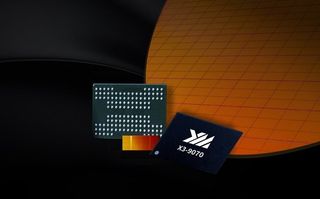
Xtacking 3.0 promo image

(Image credit: YMTC)

While in general Chinese chipmakers struggle to successfully rival established players, there are a few exceptions. YMTC (Yangtze Memory Technology Co.) is perhaps the most widely known one, a 3D NAND memory manufacturer that successfully competes against offerings from well-known producers. But to become competitive,
Please, Log in or Register to view URLs content!
reports that YMTC received support from an unexpected ally, Apple.

Apple assisted YMTC in hiring engineers from established Western companies in order to improve its yields and productivity, according to the NYT report that cites three people familiar with the matter. So far, neither Apple nor YMTC have confirmed or denied the information, though the California-based consumer electronics giant is known for helping its manufacturing partners to build their operations.

YMTC's 3D NAND devices use the company's unique Xtacking architecture. That consists of two separate wafers bonded together to build ultra-dense and ultra-fast flash memory devices that can power the
Please, Log in or Register to view URLs content!
.

With Xtacking, one wafer is used to produce NAND memory arrays leveraging the most efficient 3D NAND process technology that YMTC can design. Then a second wafer is used for various peripheral logic made on the company's most efficient logic process technology. Once the memory arrays and logic are connected using metal TSVs (through silicon vias), the resulting NAND can offer the best of both worlds: ultra-dense memory arrays and a very fast interface.

YMTC's rivals produce memory arrays and peripheral logic on the same wafer, which makes it harder for them to push their interface speeds to the limits. That in turn
Please, Log in or Register to view URLs content!
.

Making 3D NAND the way YMTC does is somewhat harder than making memory using traditional methods employed by Kioxia and Western Digital, Samsung, SK Hynix, and Micron. YMTC's 3D NAND suffered from low yields (according to media reports) and a slow ramp up, so apparently Apple helped the Chinese companies to hire engineers from reputable manufacturers to fix its issues.

For Apple, which uses 3D NAND across the vast majority of its products, it's important to diversify its supply as it helps to get better prices from each manufacturer. Helping YMTC to ramp up production means there will be more 3D NAND devices to choose from, at lower prices. Meanwhile, now that the U.S. administration has imposed severe sanctions against Chinse semiconductor and supercomputer industries, it looks like Apple no longer plans to use YMTC's 3D NAND even for its products bound to be sold in China.

YMTC became widely known by the general public after it was
Please, Log in or Register to view URLs content!
in the U.S. Department of Commerce's Unverified List in early October. The U.S. DoC's UVL includes entities whose bona fides (end users) could not be identified "satisfactorily for reasons outside the U.S. Government's control." If YMTC cannot prove to the DoC that its memory is not used by the Chinese military or security forces within 60 days after inclusion into the list, the DoC can include the company in its entity list. That would require American companies to obtain a special export license to sell their products to YMTC.

Meanwhile, four leading makers of wafer fab equipment have already
Please, Log in or Register to view URLs content!
due to
Please, Log in or Register to view URLs content!
imposed by the U.S. government in October. We've reached out to Apple and YMTC for comment and will update if we receive any further details.
 

tphuang

Lieutenant General
Staff member
Super Moderator
VIP Professional
Registered Member
Regarding the recent move by Huahong to raise money and enter Shanghai stock exchange
Please, Log in or Register to view URLs content!
12英寸扩产是公司长期规划,“8+12”战略推动其从8英寸平台向12英寸平台不断扩张,赋予强劲成长动力。截至2022年6月30日,华虹无锡12英寸晶圆厂产能已达6.5万片/月,产能利用率高达109.3%,彰显下游强劲需求。此次拟在科创板上市,募集125亿元进行无锡第二个12英寸晶圆厂扩产项目,项目预计总投资67亿美元。新建生产厂房预计2023年初开工,2024年四季度基本完成厂房建设并开始安装设备,2025年开始投产,产能逐年增长,预计最终达到8.3万片/月。华虹无锡第二个12英寸晶圆厂的扩产,将带来长期成长动力。
This is great. So, at end of Q2, we know from earnings call that they were up to 65k 12 inch wpm at Wuxi fab and that they were looking to expand it to 95k wpm.

Now, we have confirmation that the money they just got is for a second 12-inch fab at Wuxi. They are footing 12.5 billion RMB from the stock sales for this expansion, but the entire project will cost $6.7 billion. It will start construction in 2023 and start production in 2025 and eventually reaching 83k wpm. Again, that is a huge capacity. Wuxi fab produces a lot of industrial and auto power chips.

previous earnings call
Please, Log in or Register to view URLs content!
新产能,30K,释放时间?
年底前。很多设备最近已经到厂,我们持续安装,Q3、Q4可能看到12寸产能增长,为明年准备好。明年会有95K。我们认为会很快打满且爬坡很快
So, they are going from 65k wpm at end of Q2 to 95k sometimes next year and then bringing that new fab online in 2025. Overall, going from 65k wpm to 180 wpm for 12-inch wafers in probably 4 years. Huge expansion. This doesn't include their other 12-inch fabs with HLMC
 

tokenanalyst

Brigadier
Registered Member

Jingce Electronics: The company's semiconductor wafer stress measurement equipment has obtained customer orders​


Jiwei.com News Recently, Jingce Electronics said in an agency survey that at present, Shanghai Jingce, a subsidiary of the company, mainly focuses on the field of semiconductor front-end testing equipment, and is committed to the research and development and production of semiconductor front-end measurement and testing equipment. Shanghai Jinggong's film thickness products (including independent film thickness equipment) and electron beam measurement equipment have obtained batch orders from domestic first-line customers; brightfield optical defect detection equipment has obtained breakthrough orders; OCD equipment has been verified by many first-line customers Passed, and some orders have been obtained; semiconductor silicon wafer stress measurement equipment has also obtained customer orders, and the rest of the reserved products are currently in the process of research and development, certification and expansion.

Jingce Electronics believes that with the rapid development of the electric vehicle industry, big data and artificial intelligence, the demand for chip output is increasing day by day, and the domestic demand for semiconductor equipment is strong, and there will still be a relatively long continuous growth cycle in the future; at the same time, the company In the field of semiconductor testing equipment, especially in the field of front-end measurement, the supply rate of domestic equipment for production lines is relatively low. The company's main products have been recognized by many first-line customers and have achieved good market reputation. At the same time, the company is also stepping up the rest of the core. Product development, certification and expansion, so the company maintains a positive and optimistic attitude towards future sales growth in the semiconductor field.

Regarding the company's business in the fields of display, semiconductor and new energy, Jingce Electronics said that in the field of display testing, the company has continuously made breakthroughs and innovations, actively adjusted its product structure, and increased the number of panel mid- and front-end process equipment, key core devices and Micro-LEDs. , Mini-LED and other new display products research and development efforts, at the same time, the company is also constantly optimizing the customer structure, from the original focus on key customers to gradually transform into a strategic partner of large customers, to increase the expansion of overseas customers. The company has made great progress in the field of AR/VR/MR and other head-mounted display equipment supporting testing, and orders from international top strategic customers continue to increase. In the future, the company will continue to increase its research and development efforts in the field of new displays, and further increase its cooperation with leading strategic customers at home and abroad.

In the field of semiconductors, as the company's R&D investment has entered the harvest period, significant progress has been made in terms of technology, products and markets. Product maturity and market recognition of the company's products have been continuously improved, and orders have grown rapidly. From January to September 2022, the company achieved sales revenue of 112.2259 million yuan in the entire semiconductor sector, a year-on-year increase of 43.71%.

In the field of new energy, Changzhou Jingce New Energy Technology Co., Ltd. (hereinafter referred to as "Changzhou Jingce"), a subsidiary of Jingce Electronics, participated in the Hong Kong stock market of China Innovation Aviation Technology Co., Ltd. (hereinafter referred to as "China Innovation Aviation") as a cornerstone investor. Issue, further consolidate and deepen the strategic cooperative relationship between the two parties, give full play to the advantages of the two parties in resource integration, technical support, business synergy, etc., and further promote the two parties to carry out in-depth cooperation in the field of lithium battery equipment.

In addition, Jingce Electronics is actively developing cooperative relations with other well-known domestic battery manufacturers. From January to September 2022, the company achieved sales revenue of 222.7568 million yuan in the field of new energy, a year-on-year increase of 502.46%. Sales revenue and gross profit margin in the semiconductor and new energy fields continued to grow, becoming the company's new performance growth point. The company and core management members are full of confidence in the future development.

Please, Log in or Register to view URLs content!
 
Status
Not open for further replies.
Top