Chinese semiconductor industry

Status
Not open for further replies.

supersnoop

Major
Registered Member

U.S. curbs export of more AI chips, including Nvidia H800, to China​

PUBLISHED TUE, OCT 17 20238:45 AM EDTUPDATED MOMENTS AGO
thumbnail

Please, Log in or Register to view URLs content!

  • The U.S. Department of Commerce announced Tuesday that it planned to curb the sale of more advanced artificial intelligence chips to China.
  • The new export restrictions will restrict the export of Nvidia’s A800 and H800 chips, senior administration officials said.
  • The restrictions could also affect chips sold by Intel and AMD. Other rules will likely hamper the sale and export to China of semiconductor manufacturing equipment from companies such as Applied Materials, Lam and KLA.

  • U.S. curbs export of more AI chips, including Nvidia H800, to China
    Please, Log in or Register to view URLs content!

A ban on nVidia will actually hurt the US’ goals in the long run.

I asked not too long ago, why is AMD Instinct line not more popular? The answer was, simply put, they do not have the programming tool like CUDA and no one wants to develop their own because it is too time consuming…

Now by increasing the number of restrictions on these chips, you are making a CUDA alternative more and more viable. Once it is more mature, then there is no point in using nVidia's ecosystem. nVidia's performance advantage may remain on a raw chip basis, but should the system be crippled as a whole, then this leaves a gap to be filled.

Perhaps the government also believes that American companies can take a technological lead in AI and ML programming due to the performance gap, but again this kind of attempted kneecapping could lead to surprising programming creativity.

display industry supply chain used to be bread and butter for Japan .. China completed entire supply chain in just few years. BOE and other display makers mostly using domestic materials and tools.

The Japanese government through Japan Innovation Fund had sunk untold billions into propping up JDI and JOLED, JOLED is insolvent and sold all equipment to TCL/CSOT. JDI has not made a profit in many years and will likely die. Sharp had already sold to Foxconn and will likely close at some point as losses

Please, Log in or Register to view URLs content!
 

tokenanalyst

Brigadier
Registered Member

The Institute of Microelectronics has made important progress in new nanometer gate-all-around CMOS technology and device technology​

As integrated circuit manufacturing technology continues to evolve, stacked nanosheets GAA FETs will replace traditional fin transistors ( FinFETs ) at nodes below 3 nanometers , further promoting the development of the semiconductor industry. However, in the face of the demand for large-scale manufacturing, GAA transistor technology still needs to break through key challenges such as serious mismatch in operating current ( I on ) between N -type and P -type devices and difficulty in regulating threshold voltage ( V th ). It is also important for nanosheet channel materials and High- κ metal gate materials put forward more technological innovation requirements. Therefore, device structure innovation for GAA transistors has become an important direction for future logic device process research.
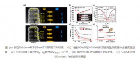
  Recently, the team of researcher Yin Huaxiang from the Leading Center of the Institute of Microelectronics adjusted the Ge content of the bottom SiGe layer in the epitaxial SiGe/Si stack on the bulk silicon substrate based on the mainstream GAA transistor manufacturing process , and used nanometer-scale high-density silicon in the back gate channel. Using SiGe layer etching technology, a GAA device ( FishboneFET ) with a channel structure similar to a fishbone was designed and prepared for the first time . Due to the introduction of additional strained SiGe nano-fin structures between traditional stacked Si nanosheets, the channel conductive area in GAA devices is greatly increased and the driving performance of P- type devices is improved under the same planar projected area . Compared with the same type of tree -like GAA device ( TreeFET ), the designed FishboneFET further improves the electrical performance mismatch problem between N -type and P -type devices, and uses a single work function metal gate material to achieve CMOS- oriented The threshold regulation of the device solves the key challenge of FishboneFET transistor in CMOS integration. Based on the above innovative technologies, the research team successfully developed CMOS FishboneFET and TreeFET devices that are compatible with mainstream GAA device processes for the first time in the world , achieving a high N/PFET device current switching ratio and a more balanced N- type under a single work function metal gate. Matching the driving performance of P -type GAA devices, it was found that N -type TreeFET and FishboneFET have more advantages in suppressing the drain-induced barrier lowering ( DIBL ) effect of short-channel devices, and TreeFET has a lower DIBL effect than FishboneFET . The research team proposed the valence band compensation theory in strained SiGe nano-fin , successfully explained the special electrical effects in the new structure, and established a key technology path for the introduction of new GAA transistors into high-performance CMOS integrated circuit applications.
  The results were recently published in the Institute of Electrical and Electronics Engineers Electronic Devices Letters ( IEEE Electron Device Letters, Vol. 44, No. 9, 1396 (2023), DOI: 10.1109/LED.2023.3294545 ), and became the " Editors' Picks " recommended and judged by the editor-in-chief of EDL , Ph.D. of the Leading Center of the Institute of Microelectronics Cao Lei is the first author of this article. Researcher Yin Huaxiang and young researcher Zhang Qingzhu are the corresponding authors of this article. This research was supported by the Strategic Priority Project ( Category A ) of the Chinese Academy of Sciences, the National Natural Science Foundation of China and other projects.


1697554439288.png
Please, Log in or Register to view URLs content!
 

measuredingabens

Junior Member
Registered Member

The Institute of Microelectronics has made important progress in new nanometer gate-all-around CMOS technology and device technology​

As integrated circuit manufacturing technology continues to evolve, stacked nanosheets GAA FETs will replace traditional fin transistors ( FinFETs ) at nodes below 3 nanometers , further promoting the development of the semiconductor industry. However, in the face of the demand for large-scale manufacturing, GAA transistor technology still needs to break through key challenges such as serious mismatch in operating current ( I on ) between N -type and P -type devices and difficulty in regulating threshold voltage ( V th ). It is also important for nanosheet channel materials and High- κ metal gate materials put forward more technological innovation requirements. Therefore, device structure innovation for GAA transistors has become an important direction for future logic device process research.
  Recently, the team of researcher Yin Huaxiang from the Leading Center of the Institute of Microelectronics adjusted the Ge content of the bottom SiGe layer in the epitaxial SiGe/Si stack on the bulk silicon substrate based on the mainstream GAA transistor manufacturing process , and used nanometer-scale high-density silicon in the back gate channel. Using SiGe layer etching technology, a GAA device ( FishboneFET ) with a channel structure similar to a fishbone was designed and prepared for the first time . Due to the introduction of additional strained SiGe nano-fin structures between traditional stacked Si nanosheets, the channel conductive area in GAA devices is greatly increased and the driving performance of P- type devices is improved under the same planar projected area . Compared with the same type of tree -like GAA device ( TreeFET ), the designed FishboneFET further improves the electrical performance mismatch problem between N -type and P -type devices, and uses a single work function metal gate material to achieve CMOS- oriented The threshold regulation of the device solves the key challenge of FishboneFET transistor in CMOS integration. Based on the above innovative technologies, the research team successfully developed CMOS FishboneFET and TreeFET devices that are compatible with mainstream GAA device processes for the first time in the world , achieving a high N/PFET device current switching ratio and a more balanced N- type under a single work function metal gate. Matching the driving performance of P -type GAA devices, it was found that N -type TreeFET and FishboneFET have more advantages in suppressing the drain-induced barrier lowering ( DIBL ) effect of short-channel devices, and TreeFET has a lower DIBL effect than FishboneFET . The research team proposed the valence band compensation theory in strained SiGe nano-fin , successfully explained the special electrical effects in the new structure, and established a key technology path for the introduction of new GAA transistors into high-performance CMOS integrated circuit applications.
  The results were recently published in the Institute of Electrical and Electronics Engineers Electronic Devices Letters ( IEEE Electron Device Letters, Vol. 44, No. 9, 1396 (2023), DOI: 10.1109/LED.2023.3294545 ), and became the " Editors' Picks " recommended and judged by the editor-in-chief of EDL , Ph.D. of the Leading Center of the Institute of Microelectronics Cao Lei is the first author of this article. Researcher Yin Huaxiang and young researcher Zhang Qingzhu are the corresponding authors of this article. This research was supported by the Strategic Priority Project ( Category A ) of the Chinese Academy of Sciences, the National Natural Science Foundation of China and other projects.


View attachment 120172
Please, Log in or Register to view URLs content!
Good to see that solid progress is being made in GAA. It will probably be a few years until SMIC can implement a 3nm or 2nm GAA process along with domestic EUV, but seeing research with successful examples is always nice. I will echo @tonyget here and ask if GAA can be manufactured by SMIC on 7nm. I'm aware Samsung has done experiments with 7nm GAA and obtained substantial performance improvements and from what I've read GAA processes don't really differ from FinFET as far as equipment goes.
 

olalavn

Senior Member
Registered Member
Tianjun-2 GPU takes the lead in adapting to Tongxin UOS and complies with UHQL specifications

Comply with localization substitution requirements. It adopts Pangu microarchitecture, with up to 1024 computing cores, and is equipped with 64-bit GDDR6 video memory, with a maximum capacity of 8GB, an equivalent frequency of 16GHz, and a bandwidth of 128GB/s.

Tianjun-2 GPU supports all mainstream graphics APIs, including DirectX, Vulkan, OpenGL, OpenCL, and VA-API

F8pevcaakAApi5B.pngF8pezfkbwAEAKRI.png
 

tokenanalyst

Brigadier
Registered Member

The Institute of Microelectronics has made important progress in new nanometer gate-all-around CMOS technology and device technology​

As integrated circuit manufacturing technology continues to evolve, stacked nanosheets GAA FETs will replace traditional fin transistors ( FinFETs ) at nodes below 3 nanometers , further promoting the development of the semiconductor industry. However, in the face of the demand for large-scale manufacturing, GAA transistor technology still needs to break through key challenges such as serious mismatch in operating current ( I on ) between N -type and P -type devices and difficulty in regulating threshold voltage ( V th ). It is also important for nanosheet channel materials and High- κ metal gate materials put forward more technological innovation requirements. Therefore, device structure innovation for GAA transistors has become an important direction for future logic device process research.
  Recently, the team of researcher Yin Huaxiang from the Leading Center of the Institute of Microelectronics adjusted the Ge content of the bottom SiGe layer in the epitaxial SiGe/Si stack on the bulk silicon substrate based on the mainstream GAA transistor manufacturing process , and used nanometer-scale high-density silicon in the back gate channel. Using SiGe layer etching technology, a GAA device ( FishboneFET ) with a channel structure similar to a fishbone was designed and prepared for the first time . Due to the introduction of additional strained SiGe nano-fin structures between traditional stacked Si nanosheets, the channel conductive area in GAA devices is greatly increased and the driving performance of P- type devices is improved under the same planar projected area . Compared with the same type of tree -like GAA device ( TreeFET ), the designed FishboneFET further improves the electrical performance mismatch problem between N -type and P -type devices, and uses a single work function metal gate material to achieve CMOS- oriented The threshold regulation of the device solves the key challenge of FishboneFET transistor in CMOS integration. Based on the above innovative technologies, the research team successfully developed CMOS FishboneFET and TreeFET devices that are compatible with mainstream GAA device processes for the first time in the world , achieving a high N/PFET device current switching ratio and a more balanced N- type under a single work function metal gate. Matching the driving performance of P -type GAA devices, it was found that N -type TreeFET and FishboneFET have more advantages in suppressing the drain-induced barrier lowering ( DIBL ) effect of short-channel devices, and TreeFET has a lower DIBL effect than FishboneFET . The research team proposed the valence band compensation theory in strained SiGe nano-fin , successfully explained the special electrical effects in the new structure, and established a key technology path for the introduction of new GAA transistors into high-performance CMOS integrated circuit applications.
  The results were recently published in the Institute of Electrical and Electronics Engineers Electronic Devices Letters ( IEEE Electron Device Letters, Vol. 44, No. 9, 1396 (2023), DOI: 10.1109/LED.2023.3294545 ), and became the " Editors' Picks " recommended and judged by the editor-in-chief of EDL , Ph.D. of the Leading Center of the Institute of Microelectronics Cao Lei is the first author of this article. Researcher Yin Huaxiang and young researcher Zhang Qingzhu are the corresponding authors of this article. This research was supported by the Strategic Priority Project ( Category A ) of the Chinese Academy of Sciences, the National Natural Science Foundation of China and other projects.


View attachment 120172
Please, Log in or Register to view URLs content!
1697558108528.png
 

Zichan

Junior Member
Registered Member
The new tranche of export controls is closing some of the loop holes by targeting chip compute performance and not merely memory bandwidth. Any chip over 300 tera flops/s will not be allowed for export. Furthermore, chips between 170 and 300 teraflops are barred if their compute density exceeds 370 gflops/mm2.

The A800 would therefore not make the cut, as its peak compute is 312 teraflops/s.

However, what’s to stop Nvidia from making another version of the chip with lower clocks? The clients could theoretically “overclock” the chips to un-nerf the chips.

A careful examination of the export controls text should answer this.

Noteworthy, these restrictions don’t apply for consumer grade hardware like smartphones.

I like that the BIC bulletin specifies the military applications of advanced AI: cognitive electronic warfare, radar, signals intelligence, and jamming. Not exactly new to anyone familiar with the matter, but still.
 
Last edited:

tokenanalyst

Brigadier
Registered Member

The total investment is 3.457 billion yuan! Newly added annual production capacity of 700,000 pieces of 6-8 inch silicon carbide single crystal substrate project​


On October 10, the Baotou Municipal People’s Government and Hefei Century Gold Core Semiconductor Co., Ltd. officially signed a strategic cooperation agreement in Baotou City for the “Annual Production of 700,000 Pieces of 6-8-inch Silicon Carbide Single Crystal Substrate Project”.

This project is introduced with the assistance of Baotou·Beijing Science and Technology Innovation Base, and is planned to be launched in Qingshan District Equipment Manufacturing Industrial Park, Baotou City. The total investment is 3.457 billion yuan. The total project construction period is 3 years. When it is officially put into operation, it will have an annual output of 700,000 pieces6-8 The 1-inch single crystal substrate production line also includes silicon carbide single crystal growth, cutting, grinding, polishing and testing, etc., which will effectively promote the growth of the crystalline silicon industry in Qingshan District and help the equipment manufacturing park develop new crystalline silicon products.

Please, Log in or Register to view URLs content!
 

tphuang

Lieutenant General
Staff member
Super Moderator
VIP Professional
Registered Member

The total investment is 3.457 billion yuan! Newly added annual production capacity of 700,000 pieces of 6-8 inch silicon carbide single crystal substrate project​


On October 10, the Baotou Municipal People’s Government and Hefei Century Gold Core Semiconductor Co., Ltd. officially signed a strategic cooperation agreement in Baotou City for the “Annual Production of 700,000 Pieces of 6-8-inch Silicon Carbide Single Crystal Substrate Project”.

This project is introduced with the assistance of Baotou·Beijing Science and Technology Innovation Base, and is planned to be launched in Qingshan District Equipment Manufacturing Industrial Park, Baotou City. The total investment is 3.457 billion yuan. The total project construction period is 3 years. When it is officially put into operation, it will have an annual output of 700,000 pieces6-8 The 1-inch single crystal substrate production line also includes silicon carbide single crystal growth, cutting, grinding, polishing and testing, etc., which will effectively promote the growth of the crystalline silicon industry in Qingshan District and help the equipment manufacturing park develop new crystalline silicon products.

Please, Log in or Register to view URLs content!
china is going to blow away all the foreign companies in Sic production in a couple of years.
 

tokenanalyst

Brigadier
Registered Member

“Pulin Technology” received tens of millions of angel round financing​

According to news on October 9, Pulin Technology (Hangzhou) Co., Ltd. ("Pulin Technology"), a research and development company for nanoimprint equipment and materials, recently completed tens of millions of yuan in angel round financing, exclusively invested by Fengrui Capital.

Please, Log in or Register to view URLs content!
 
Status
Not open for further replies.
Top