Chinese semiconductor industry

Status
Not open for further replies.

usb

Just Hatched
Registered Member
1. Thanks for replying

The new (proposed) strategy of allowing AI GPUs like Nvidia H100s and A100s to be sold enables China to be addicted to Western software ecosystems (i.e., CUDA) and dominate domestic alternatives.
The problem with that strategy is, that they already dominate the AI GPU Market with Huawei being the only real alternative. Other domestic companies like Tencent are reluctant to switch to Huawei because they dont want to be reliant on them and unless someone like Moores Thread or Biren develops an alternative, they are unlikely to switch anyway. Other than that, it takes away the competitive advantage that US Companies have over Chinese ones and might therefore accelerate Chinas AI development (,which the US thinks it bad). It would make sense if Biren or Moores Thread were making 7nm AI Chips but they dont so the US wouldnt really gain anything from it.

Huawei isn't dumb, it will still cultivate it's domestic supply chain, but I'm sure Huawei would be interest in some chips from TSMC for global versions of Mate series. For high-end chips, Huawei can dual source SMIC and TSMC for China-only versions and Global versions of Mate series, respectively. It would allow Huawei to be competitive in overseas. Later revert to single sole source from SMIC when 3nm EUV is scaled.
That is exactly the reason why I dont see Huawei being allowed to fab at TSMC, since it would make them more competitive and therefore takes away marketshare from other companies like Samsung or Apple, meaning less profits for them and therefore less R&D (not to mention that TSMC is a Taiwanese company and not an American so the US would never allow it anyway). As you correctly pointed out, Huawei would also only ever a temporary customer and would switch back to SMIC as soon as possible and therefore bringing no real long-term advantage (unless Huawei develops "dementia" or a "forget und forgive" attitiude, but i seriously doubt it). Huawei is currently also capacity limited and I think the US wants to keep it that way for as long as possible.
 

huemens

Junior Member
Registered Member
It could also be anticipation of a strong demand of 7nm chips and 9000s variant.
Please, Log in or Register to view URLs content!
This report originated from a complete garbage source. It is the same Taiwanese site that couple of days ago claimed that SMIC made the 7nm chip by borrowing EUVs from a Chinese memory fab. This Toms Hardware guy just copied from that.
 

tokenanalyst

Brigadier
Registered Member

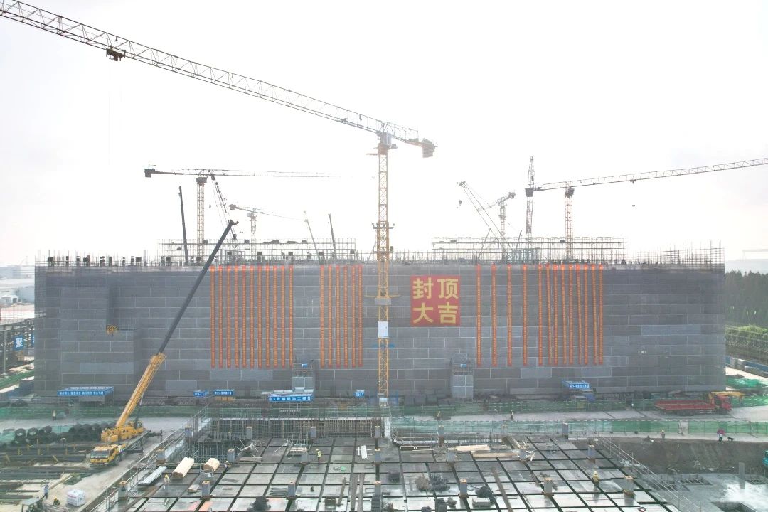
The main factory building of Jita Semiconductor’s characteristic process production line construction project (second phase) is capped​

on September 28, the main factory building of the Jita Semiconductor characteristic process production line construction project (second phase) was capped.
687963341236.2615.jpg

Image source: China Construction Eighth Engineering Bureau Development and Construction Company
Zhang Rujing, executive director of Jita Semiconductor Co., Ltd., said that the capping of the main factory building has laid a solid foundation for the completion of the project. Jita Semiconductor Co., Ltd. will forge ahead and continuously improve the level of technological innovation to solve the technical problems of high-end automotive chip manufacturing and promote the domestic chip industry. make greater contributions to development.


Please, Log in or Register to view URLs content!
 

tokenanalyst

Brigadier
Registered Member

QiMoor completed Pre-A round financing of 100 million yuan to accelerate the layout of high-performance interconnected chips​


Recently, Qimoor announced the completion of Pre-A round financing of 100 million yuan, led by the China State-owned Enterprise Mixed Ownership Reform Fund (Mixed Reform Fund). The main investors include Zhongguancun Development Qihang Investment, Lirong Yuanchang, Rice Growth, Jinnan Haihe Smart Selection, Junhao Hongshi, etc. This round of funds will be mainly used for the next generation of high-performance interconnect chips (chiplets), network acceleration chip technology research and development, team expansion and market promotion.
QiMoor is a high-performance interconnect products and solutions company. Based on the Kiwi-Link unified interconnect architecture, Kiwi provides full-link interconnect and network acceleration core products and solutions to help high-performance computing customers build ultra-large-scale distributed intelligent computing platforms more efficiently and at lower costs. Its core products include 2.5D IO Die, 3D Base Die and other high-performance interconnect cores, network acceleration cores and a full range of Die2Die IP.
According to official news from QiMoore, the industry's first "high-performance interconnected chip 3D Base Die" developed by the company based on the 3D Chiplet architecture is officially tape-out and planned to be released within the year.

Please, Log in or Register to view URLs content!
 

tokenanalyst

Brigadier
Registered Member

To accelerate the efficiency of lithography OPC, Tencent submitted a patent application for a mask generation model training method​

Tencent Technology (Shenzhen) Co., Ltd. recently submitted an invention patent application titled "Mask generation model training method, mask generation method and device and storage medium", application number CN202311005424.2, public number CN116720479A.
According to the patent text, as the feature size of very large-scale integrated circuits continues to shorten and is lower than the wavelength of the light source used in the photolithography process, interference and diffraction phenomena are very obvious, causing the pattern exposed on the wafer through the mask to be different from that of the light source used in the photolithography process. The required patterns are very different, which greatly affects the performance, production capacity and yield of the chip. In order to solve this problem, deep learning technology has been applied to various fields of chip design and manufacturing. In order to ensure high quality of the mask, it is necessary to ensure that the complexity of the generated mask is low. The embodiments of this application provide a mask generation model training method, a mask generation method and device, and a storage medium, which can reduce the complexity of the mask.
The patented method described in the patent includes: obtaining a training sample set, a training sample including a target layout of the chip sample and a mask of the target layout, and for at least one training sample, using the target layout of the chip sample as the input of the mask generation model, Obtain the predicted mask of the target layout, input the predicted mask of the target layout into the lithography physical model, and obtain the wafer pattern corresponding to the predicted mask. The kernel function is passed through the intersection of the lithography system (such as the 193-nanometer ring light source) The transfer coefficient is obtained by singular value decomposition. According to the sum of the perimeters of multiple graphics included in the target layout of the chip sample and the perimeter of the predicted mask of the target layout, determine the complexity of the predicted mask of the target layout. According to the target layout of the chip sample, the predicted mask of the target layout corresponds The wafer pattern, the mask of the target layout, the predicted mask of the target layout, and the complexity of the predicted mask of the target layout are adjusted. The parameters of the mask generation model are adjusted until the conditions for stopping training are met and the trained mask is obtained. Generate models.

Please, Log in or Register to view URLs content!
 

supersnoop

Major
Registered Member
Please, Log in or Register to view URLs content!

review here of Matepad pro 13.2 made me realize that Kirin 9000S really needs to support a lot, since it needs to be optimized for phone and tablet.

Tablet requirements for video quality, sound and m-pencil are high. Since Matepad would be expected to be used as a work station in some cases. It will more often be used to watch TV and long form video.

As such, it supports the new HDR Vivid audio/video which requires higher end graphic rendering + AI (imo, it needs similar features to what Honghu-900 supports for a larger screen, but on a smaller scale). The auto correct feature on m-pencil also requires more AI.

it needs to eventually support higher end gaming, which is probably why they came out with the frame filling feature on 9000S to bring up the fps, power consumption performance.

All of which leads me to think longer term, Huawei will get into stand alone GPUs for tablet & laptops, since it wants to gain in workstation and home PC business also.

Also points to Kirin 9000S having to be jack of all trade in some ways to support Mate 60, 5X and Pad. Next gen, I'd imagine they need dedicated Kirin chips for tablet, higher end phone, lower end phone and laptops. Expect this to be the first step in Huawei achieving full range of phone to server CPU/GPU/SoC/NPU. It's main limitations are what SMIC can fab, but that does drive innovation on Huawei design, optimization & firmware.

Why would you go into stand alone GPU, especially for laptops? Standalone GPU market is a dead end for consumer/end user space, how many computers are sold with standalone GPUs? Even for higher end gaming you can build an integrated chip with high performance GPU like Apple. No point in targeting the xx70-series and above (nVidia, x600 for AMD), they are niche products.

GPU and NPU will be integrated, even in a datacenter setting, it will likely be in non standard format with a custom high speed interconnect and just sold as a cloud service. This is the most logical business wise
 

Proton

Junior Member
Registered Member
Why would you go into stand alone GPU, especially for laptops? Standalone GPU market is a dead end for consumer/end user space, how many computers are sold with standalone GPUs? Even for higher end gaming you can build an integrated chip with high performance GPU like Apple. No point in targeting the xx70-series and above (nVidia, x600 for AMD), they are niche products.

GPU and NPU will be integrated, even in a datacenter setting, it will likely be in non standard format with a custom high speed interconnect and just sold as a cloud service. This is the most logical business wise
Nvidia has a market cap of $1 trillion.
 

tphuang

Lieutenant General
Staff member
Super Moderator
VIP Professional
Registered Member
Why would you go into stand alone GPU, especially for laptops? Standalone GPU market is a dead end for consumer/end user space, how many computers are sold with standalone GPUs? Even for higher end gaming you can build an integrated chip with high performance GPU like Apple. No point in targeting the xx70-series and above (nVidia, x600 for AMD), they are niche products.

GPU and NPU will be integrated, even in a datacenter setting, it will likely be in non standard format with a custom high speed interconnect and just sold as a cloud service. This is the most logical business wise
because there is clearly a market there. And more importantly, Huawei SoC does not have the luxury of using TSMC 3nm process. If it wants to use its own chips for a "computer" that is used for demanding graphics in the future, then its current SoC is not suitable for that job

seriously, got watch the geekerwan video.
 

tokenanalyst

Brigadier
Registered Member

Tianyue Advanced's revenue in the first three quarters increased by 178.31%-200.57%​


On September 26, Tianyue Advanced released its performance forecast for the first three quarters of 2023, stating that it expected to achieve operating income of 750 million yuan to 810 million yuan, compared with 269.4847 million yuan in the same period last year, a year-on-year increase of 178.31% to 200.57%.

At the same time, data shows that Tianyue Advanced achieved operating income of 269.4847 million yuan in the first three quarters of 2022.

Tianyue Advanced stated on the main reasons for the changes in operating data in this period that Tianyue Advanced's operating income increased significantly year-on-year during the reporting period. This was mainly due to strong downstream market demand during the reporting period. Tianyue Advanced's orders were sufficient. As the company's conductive product production capacity continued Improvement, Tianyue's advanced product delivery capabilities continue to rise.

Tianyue Advanced is a leading domestic manufacturer of wide bandgap semiconductor materials. It is currently mainly engaged in the research and development, production and sales of silicon carbide semiconductor materials. Its products can be widely used in microwave electronics, power electronics and other fields. Wide bandgap semiconductor materials have clear and considerable market prospects in 5G communications, new energy vehicles, energy storage and other fields, and are an important development direction for the semiconductor industry.

In terms of products, Tianyue Advanced has achieved large-scale supply of 6-inch conductive substrates, 6-inch semi-insulating substrates, 4-inch semi-insulating substrates and other products. Tianyue's advanced and high-quality 6-inch products have been widely recognized by downstream customers in the industry. In terms of 8-inch product layout, Tianyue Advanced has the ability to mass-produce 8-inch products. In the first half of the year, it has carried out customer sample verification and achieved small batch sales. It is expected that the scale of production and sales will continue to expand.

Please, Log in or Register to view URLs content!
 

tokenanalyst

Brigadier
Registered Member

JACS: Tsinghua team has made important progress in the research and development of ultra-high sensitivity photoresist​


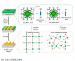
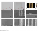
Photoresist is a key material for the large-scale manufacturing of integrated circuit chips. After the technology has developed to the deep ultraviolet (DUV) and extreme ultraviolet (EUV) lithography stages, photoresist is not sensitive enough to light sources, which has greatly pushed up the cost of lithography. The difficulty and cost of manufacturing the machine and its supporting light source. Recently, the New Energy and Materials Chemistry Team of the Institute of Nuclear and New Energy Technology of Tsinghua University combined efficient mercapto-ethylene click chemistry technology with multifunctional metal oxide nanocluster photoresist technology, and proposed "click lithography" for the first time in the world. "New ideas, new methods, and successfully produced ultra-high sensitivity photoresist samples. Photolithography test results from international authoritative organizations show that this material can achieve high-contrast imaging at extremely low exposure doses. The highest sensitivity in deep UV lithography is 7.5 mJ cm-2, and the required exposure dose is reduced by about 20 times compared with traditional photoresist systems.
At the same time, dense patterns with a line width resolution of 45 nm were obtained by low-dose electron beam lithography (10-40 μC cm -2), demonstrating its ability to be applied to high-resolution lithography. Next, the author also conducted a preliminary study on the post-processing properties, etching resistance and pattern transfer capabilities of the prepared zirconia photoresist based on click reaction.

1696257916507.png1696257948329.png

Please, Log in or Register to view URLs content!
 
Status
Not open for further replies.
Top