Chinese semiconductor industry

Status
Not open for further replies.

no_name

Colonel
Apparently China is using a different approach to producing 5nm chips from companies like ASML, who focused on very complex solutions because they need to sell lithography machines as products which demand compactness.

China is adopting a 'production line' approach which is more expensive to set up, takes up more space, and uses more power, but this is a trade off they were willing to make because their primary concern now is not to sell products but to ensure they can make their own chips.

In very simplified terms, ASML uses a very complex setup to produce beams and filter for the right frequency to etch their chips. the Chinese method instead produces a more messy beam but had it run through a much longer 'track'. Over a long distance the beams of different wavelengths will disperse differently and become separated more, and then it is just a matter of capturing the beam of the right wavelength at the right placement for etching.

Advantage of this is that they can run multiple chips sizes at once (28, 20, 16, 10, 9, 7, 5mm etc) and apparently can also select for 3mm, 1mm and even up to 0.1mm, if other physics factors are not prevent it already.

And apparently rejects from say a finer transistor size run might be able to be re-etched at a coarser size for other purposes.

China is not making lithography machines. She is building lithography factories. The kind of stuff that even ASML might not be able to pull off but China had the resource and the necessity to make happen.
 
Last edited:

coolgod

Colonel
Registered Member
Apparently China is using a different approach to producing 5nm chips from companies like ASML, who focused on very complex solutions because they need to sell lithography machines as products which demand compactness.

China is adopting a 'production line' approach which is more expensive to set up, takes up more space, and uses more power, but this is a trade off they were willing to make because their primary concern now is not to sell products but to ensure they can make their own chips.

In very simplified terms, ASML uses a very complex setup to produce beams and filter for the right frequency to etch their chips. the Chinese method instead produces a more messy beam but had it run through a much longer 'track'. Over a long distance the beams of different wavelengths will disperse differently and become separated more, and then it is just a matter of capturing the beam of the right wavelength at the right placement for etching.

Advantage of this is that they can run multiple chips sizes at once (28, 20, 16, 10, 9, 7, 5mm etc) and apparently can also select for 3mm, 1mm and even up to 0.1mm, if other physics factors are not prevent it already.

And apparently rejects from say a finer transistor size run might be able to be re-etched at a coarser size for other purposes.

China is not making lithography machines. She is building lithography factories. The kind of stuff that even ASML might not be able to pull off but China had the resource and the necessity to make happen.
This isn't a ELI5 thread. I don't understand your analogy at all, exactly which technology are you trying to explain?
 

sndef888

Captain
Registered Member
This isn't a ELI5 thread. I don't understand your analogy at all, exactly which technology are you trying to explain?
SSMB EUV.

There's been a lot of speculation about it on Chinese socmed for a couple days, but I have no idea whether it's legit or not.

I kind of recall seeing someone posting that the SSMB EUV produced by Tsinghua was not high power enough (or something) on this forum
 

coolgod

Colonel
Registered Member
SSMB EUV.

There's been a lot of speculation about it on Chinese socmed for a couple days, but I have no idea whether it's legit or not.

I kind of recall seeing someone posting that the SSMB EUV produced by Tsinghua was not high power enough (or something) on this forum
I don't think his analogy was a very illuminating explanation for SSMB EUV technology. His analogy makes it seem like SSMB EUV is just taking radiation from a synchrotron and filtering the specific wavelength by letting the light naturally disperse through a long enough track. I also don't think the SSMB EUV machine can filter out multiple different frequencies simultaneously to produce different nm chips.

From my brief reading of the Tsinghua slides, I don't think this is how SSMB EUV works. The difficulty and novelty isn't getting the synchrotron light source or filtering the output radiation. The core part of the technology is using an accelerator to get the electrons in the system to be in a Steady State (i.e., continuous operation) and for them to be MicroBunching (i.e., to produce narrow band coherent light).
 
Last edited:

coolgod

Colonel
Registered Member
Apparently China is using a different approach to producing 5nm chips from companies like ASML, who focused on very complex solutions because they need to sell lithography machines as products which demand compactness.

China is adopting a 'production line' approach which is more expensive to set up, takes up more space, and uses more power, but this is a trade off they were willing to make because their primary concern now is not to sell products but to ensure they can make their own chips.

In very simplified terms, ASML uses a very complex setup to produce beams and filter for the right frequency to etch their chips. the Chinese method instead produces a more messy beam but had it run through a much longer 'track'. Over a long distance the beams of different wavelengths will disperse differently and become separated more, and then it is just a matter of capturing the beam of the right wavelength at the right placement for etching.

Advantage of this is that they can run multiple chips sizes at once (28, 20, 16, 10, 9, 7, 5mm etc) and apparently can also select for 3mm, 1mm and even up to 0.1mm, if other physics factors are not prevent it already.

And apparently rejects from say a finer transistor size run might be able to be re-etched at a coarser size for other purposes.

China is not making lithography machines. She is building lithography factories. The kind of stuff that even ASML might not be able to pull off but China had the resource and the necessity to make happen.
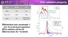
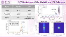
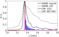
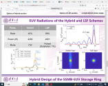
To drive the point home why his analogy is not good. These are the (theoretical?) output spectra from SSMB EUV light source, at 13.5nm of course to reuse the existing EUV lithography infrastructure.

1694835823781.png
1694835841486.png

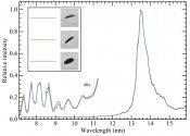
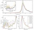
Compared to the experimental output spectra from existing ASML EUV source.

1694835934564.jpeg1694836035396.jpegSource:
Please, Log in or Register to view URLs content!

This figure in the Tsinghua slides already give a comparison between the spectra of the proposed SSMB schemes with the existing laser-produced plasma (LPP) sources, i.e., ASML EUV = LPP: CO2. Though to be fair it is comparing theoretical values with experimental data.

1694836995354.png
At least from the frequency spectra of the EUV sources I would not characterize the SSMB EUV beam as more "messy". The whole point of the MicroBunching is to generate a very "clean" light.
 

Attachments

  • 1694835784437.png
    1694835784437.png
    509.7 KB · Views: 5
Last edited:

coolgod

Colonel
Registered Member
I took a look on Chinese internet and just like the LK-99 hoax, there were tons of SSMB EUV misinformation floating on the internet. Does anyone actually know the biggest bottle necks on why China can't produce EUV lithography machines? I suspect intellectual property rights play a large role on why China can't just make a machine similar to ASML EUV lithography using mostly domestic equipment in a short period of time.

Chinese EUV lithography machine manufactures have to devise methods that are sufficiently different from the ASML EUV lithography machine and its subsystems (if China still wants to respects ASML IP) but still performs in the same ballpark. I think this additional difficulty from IP rights is one of the reasons why the SSMB EUV pathway seems so attractive.
 
Last edited:

latenlazy

Brigadier
Apparently China is using a different approach to producing 5nm chips from companies like ASML, who focused on very complex solutions because they need to sell lithography machines as products which demand compactness.

China is adopting a 'production line' approach which is more expensive to set up, takes up more space, and uses more power, but this is a trade off they were willing to make because their primary concern now is not to sell products but to ensure they can make their own chips.

In very simplified terms, ASML uses a very complex setup to produce beams and filter for the right frequency to etch their chips. the Chinese method instead produces a more messy beam but had it run through a much longer 'track'. Over a long distance the beams of different wavelengths will disperse differently and become separated more, and then it is just a matter of capturing the beam of the right wavelength at the right placement for etching.

Advantage of this is that they can run multiple chips sizes at once (28, 20, 16, 10, 9, 7, 5mm etc) and apparently can also select for 3mm, 1mm and even up to 0.1mm, if other physics factors are not prevent it already.

And apparently rejects from say a finer transistor size run might be able to be re-etched at a coarser size for other purposes.

China is not making lithography machines. She is building lithography factories. The kind of stuff that even ASML might not be able to pull off but China had the resource and the necessity to make happen.
SSMB EUV.

There's been a lot of speculation about it on Chinese socmed for a couple days, but I have no idea whether it's legit or not.

I kind of recall seeing someone posting that the SSMB EUV produced by Tsinghua was not high power enough (or something) on this forum
This isn’t how SSMB works. All synchrotron methods are tuned to generate single wavelength emissions. The way synchrotron light sources work is by accelerating electrons until they’ve reached a certain speed, and then braking them, which causes the electrons to emit the energy they lose as radiation of a specific wavelength defined by the difference in speed between their two velocities. Because a scanner needs a constant stream of photons to work as a scanner, you would normally need a very large accelerator to provide the stream of electrons need to provide long enough scanning exposure for the energies needed to generate light emissions at EUV wavelengths at outputs useful for industrial photolithography. SSMB is supposed to solve this by accelerating electrons in bunches, allowing you to increase the power density and frequency of your light generation with a much smaller accelerator ring. But ultimately the scanning process is still using only one wavelength. You can split the ring into multiple scan points though, with electrons accelerating and then decelerating before each scan point. In that sense you can build an assembly line for scanning.

Unrelated to SSMB but a traditional scanner doesn’t use filters either. They’re also single wavelength light sources. That’s why before EUV the light sources were all lasers. LPP based EUV light sources diverge a little in that the light generated from exciting tin plasma with a drive laser aren’t all in the 13.5 nm wavelength you want. But the photons that sit outside that wavelength aren’t “filtered” so much as lost as the light beam is passed through a number of reflective optical passes.
 

latenlazy

Brigadier
I took a look on Chinese internet and just like the LK-99 hoax, there were tons of SSMB EUV misinformation floating on the internet. Does anyone actually know the biggest bottle necks on why China can't produce EUV lithography machines? I suspect intellectual property rights play a large role on why China can't just make a machine similar to ASML EUV lithography using mostly domestic equipment in a short period of time.

Chinese EUV lithography machine manufactures have to devise methods that are sufficiently different from the ASML EUV lithography machine and its subsystems (if China still wants to respects ASML IP) but still performs in the same ballpark. I think this additional difficulty from IP rights is one of the reasons why the SSMB EUV pathway seems so attractive.
This speculation is also misinformation. The constraint is not IP. The engineering and physics involved in this technology is just very difficult. In addition to SSMB China is currently also developing LPP based light sources using the same mechanisms as ASML (and also Gigaphoton).
 

coolgod

Colonel
Registered Member
This speculation is also misinformation. The constraint is not IP. The engineering and physics involved in this technology is just very difficult. In addition to SSMB China is currently also developing LPP based light sources using the same mechanisms as ASML (and also Gigaphoton).
I know that engineering involved is difficult but I'm wondering would IP play a large role as design constraints? If we ignore the IP aspect, did China in 2020 really not have the technical capabilities to reverse engineer each component in ASML's EUV lithography machine?

I'm not knowledgeable about IP laws, so I speculated IP rights might be a constraint. Are you suggesting that the patents (in China) given to ASML, Gigaphoton and other foreign companies regarding EUV technologies are narrow enough such that Chinese manufacturers can design EUV lithography machines following their footsteps while making only minimal adjustments?
 

no_name

Colonel
This isn’t how SSMB works. All synchrotron methods are tuned to generate single wavelength emissions. The way synchrotron light sources work is by accelerating electrons until they’ve reached a certain speed, and then braking them, which causes the electrons to emit the energy they lose as radiation of a specific wavelength defined by the difference in speed between their two velocities. Because a scanner needs a constant stream of photons to work as a scanner, you would normally need a very large accelerator to provide the stream of electrons need to provide long enough scanning exposure for the energies needed to generate light emissions at EUV wavelengths at outputs useful for industrial photolithography. SSMB is supposed to solve this by accelerating electrons in bunches, allowing you to increase the power density and frequency of your light generation with a much smaller accelerator ring. But ultimately the scanning process is still using only one wavelength. You can split the ring into multiple scan points though, with electrons accelerating and then decelerating before each scan point. In that sense you can build an assembly line for scanning.

Unrelated to SSMB but a traditional scanner doesn’t use filters either. They’re also single wavelength light sources. That’s why before EUV the light sources were all lasers. LPP based EUV light sources diverge a little in that the light generated from exciting tin plasma with a drive laser aren’t all in the 13.5 nm wavelength you want. But the photons that sit outside that wavelength aren’t “filtered” so much as lost as the light beam is passed through a number of reflective optical passes.
That's a lot clearer now. Thanks.
 
Status
Not open for further replies.
Top