Chinese semiconductor industry

Status
Not open for further replies.

SanWenYu

Captain
Registered Member

horse

Colonel
Registered Member
What are you taking about. Definitely not all western media. BBC did not really acknowledge the news. They had a segment on how the brave Phillipines were standing up to china as David vs Goliath but failed to report the rally David vs Goliath in Huawei vs the US of A. Typical. That's why I don't put any credence in the BBC.

No Canadian media outlet has reported about Huawei Mate 60 Pro either.
 

tokenanalyst

Brigadier
Registered Member

Shanghai Belling: 3Gsps sampling rate ADC product has completed pre-research and is expected to be mass-produced within 1 year​


According to Jiwei.com, Shanghai Belling recently stated in an institutional survey that the company has completed pre-research on 3Gsps sampling rate ADC products and is expected to launch mass production products within a year. The company is developing ADC-related products with higher sampling rates.
In terms of R&D, Shanghai Belling said that in recent years, the company has continued to attach importance to R&D team building, expand the scale of the R&D team, and establish new product projects and R&D layout in the fields of industrial control and automotive electronics. In addition, Shanghai Belling said that based on market and customer needs, the company has developed a series of dedicated microcontroller SoC products in the field of optical communications and has achieved mass production. Shanghai Belling optical module SoC chips are actively introduced to multiple customers, involving wireless access, data communications, GPON, Combo PON and other application projects. Shanghai Belling has laid out SoC products dedicated to high-end optical modules for datacom, and will increase R&D investment in the future to develop higher-integrated optical module SoC products.
Shanghai Belling further pointed out that the Chinese market is the world's largest semiconductor market, and "domestic substitution" is an important driving force for the rapid development of the domestic semiconductor industry in recent years. Shanghai Belling's IC products are mainly deployed in analog circuits, and are constantly iterating to higher technical levels. At the same time, Shanghai Belling continues to launch dedicated SOC products for key market areas such as automotive electronics, industrial control energy storage, building intelligence and home appliances, and maintains a good development momentum.
In terms of new energy layout, Shanghai Belling said that the company has deployed all-round product business in the field of automotive electronics in recent years, involving power management, power devices, motor drives, EEPROM memories, isolator products, interface chips, data conversion products and other fields. The R&D layout provides a rich series of products for automotive lighting, automotive ignitions, automotive air conditioning PTC, main drive and other applications for fuel vehicles and new energy vehicles, and continues to expand other automotive electronics segmentation application platforms. At present, the number of products and revenue scale in Shanghai Belling's automotive electronics field are in a stage of rapid growth.

Please, Log in or Register to view URLs content!
 

tokenanalyst

Brigadier
Registered Member

FACING THE DIFFICULTIES, NORTHERN HUACHUANG'S METAL FILM SOLUTIONS HELP ADVANCED PACKAGING TECHNOLOGY BREAK THROUGH BOTTLENECKS​


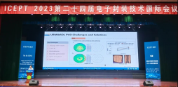
The 24th International Conference on Electronic Packaging Technology (ICEPT 2023) was successfully held at Shihezi University in Xinjiang recently. Northern Huachuang was invited to participate in the conference and met with more than 700 experts, scholars and industry experts in the field of semiconductor packaging from 14 countries and regions around the world. People from all over the world gathered together to have an in-depth discussion on advanced packaging technology innovation, academic exchanges and international cooperation.

  ICEPT is one of the flagship conferences of the International Institute of Electrical and Electronics Engineers Electronic Packaging Society (IEEE-EPS) in China. Since its inception in 1994, it has been successfully held for 23 times in Beijing, Shanghai, Shenzhen and other places, and has now become an international electronic packaging conference. One of the four major academic conferences in the field [1].
  As the size of transistors continues to approach the atomic scale, Moore's Law is slowing down. Advanced packaging, as an important way to integrate chips, has obvious advantages in reducing process costs and improving device performance. However, it also suffers from wafer warpage (Warpage). , adhesion (Adhesion), contact resistance (Rc) and other aspects have put forward higher requirements and challenges for metal interconnection equipment and processes.
  
Geng Bo, deputy general manager of Northern Huachuang's PVD business unit, gave a report titled "Integrated Solution for Metal Film Equipment" at the conference. The report starts from the innovative exploration practice of Northern Huachuang and introduces the overall solution of metal film preparation equipment for the advanced packaging field. This solution can help packaging companies break through technical bottlenecks such as warping chip transmission and loading, effectively reduce contact resistance, improve adhesion, optimize particle control capabilities, significantly improve film performance, increase production capacity, and reduce costs.

1694460748159.png

  Northern Huachuang has been deeply involved in the industry for more than 20 years, and has formed a multi-category series of products with advanced technology and reliable performance in the fields of etching, thin film deposition, oxidation/diffusion, and cleaning. Looking forward to the future, Northern Huachuang is willing to work hand in hand with industry colleagues and work together to promote continuous breakthroughs in advanced packaging technology and provide more and better solutions.

Please, Log in or Register to view URLs content!
 

Awenumick

New Member
Registered Member
I have high hopes for the SSMB EUV. I'm not an expert on particle physics, but from what I can tell, the SSMB EUV is basically a normal synchrotron that has a special array of magnetic undulators and laser that produce simulate the electrons to produce the EUV beam. But apart from the specifically built array of lasers and magnetic undulators that have to be situated next to the beamline, it's otherwise a normal synchrotron. It's not some completely brand new machine that has never been assembled before, with thousands of moving parts and a hundred thousand components. Synchrotron have been a thing since the 50s, and there's dozens of them in operation around the world today. And they can be build without ultra ultra specialised parts or companies.

And synchrotron and using them as a light source is a very mature field. Unlike ASML's EUV machine that can only really be assembled by them, around a dozen countries and companies can produce their own synchrotron and storage rings and have done so for decades. So there shouldn't be a bottleneck or lack of experience in building the majority of the synchrotron. The only bottleneck will be the special laser and magnet undulators used in actually producing the beam, but the main bulk of construction of the large machine shouldn't have any issues. Engineers and physicists also won't be in a short supply for the operation of the synchrotron, since they're a very mature technology at this point.

We might see the prototype SSMB EUV under construction get finished a lot faster than we thought, if 90% of it's construction is similar to the existing synchrotrons already in China. Hell, even if there's issues with the laser and the undulator, we might see multiple of the basic synchrotron built first and the laser/magnet undulators installed after the issues have been sorted out.

It depends on how hard it is to produce the special laser/magnet undulators how to control the laser/magnet undulators to produce the desired wavelength, but those are mainly controlled by computers/A.I which are getting better and better every year. Not to mention that undulators being used to control a synchrotron/FEL are also a very mature technology. Which is to say I can see the EUV light source being ready before the optical system, mask, EUV photoresist etc etc, with the main bottleneck being the other systems and how to integrate the EUV light source into a singular system. Like they build the synchrotron, have the laser and undulator installed, turn it on and with a few days of tweaking succeed in getting the desired EUV beam that they need.

Having the EUV light source be ready before the other components are ready could be beneficial, you could test your various photoresist, masks etc etc on the very same light source that they are designed to be integrated with.

Which would be funny if the most complicated part of a EUV machine, the light source, was the first part to be finished or one of the easiest and ASML chased after the more complicated LPP method after more than a decade just because the steady-state microbunching technique wasn't invented until 2010.
Found an interesting info regarding ssmb.
"Tsinghua's so-called SSMB light source results are only to Germany's synchrotron radiation light source for a verification, SSMB-EUV conversion rate of only 1 ‰, is not considered the ultimate "results". Only 1% of the ASML power

Tsinghua has always been unreliable

Looking forward to Tsinghua might as well look forward to the DPP-EUV light source of Harbin Institute of Technology.

That is the real hope of China"
If this is true then we are not seeing ssmb euv anytime soon.
 

tokenanalyst

Brigadier
Registered Member
Found an interesting info regarding ssmb.
"Tsinghua's so-called SSMB light source results are only to Germany's synchrotron radiation light source for a verification, SSMB-EUV conversion rate of only 1 ‰, is not considered the ultimate "results". Only 1% of the ASML power

Tsinghua has always been unreliable

Looking forward to Tsinghua might as well look forward to the DPP-EUV light source of Harbin Institute of Technology.

That is the real hope of China"
If this is true then we are not seeing ssmb euv anytime soon.
Never take whatever you read in twitter or any social media seriously. Do your own research.
 

ansy1968

Brigadier
Registered Member
I have high hopes for the SSMB EUV. I'm not an expert on particle physics, but from what I can tell, the SSMB EUV is basically a normal synchrotron that has a special array of magnetic undulators and laser that produce simulate the electrons to produce the EUV beam. But apart from the specifically built array of lasers and magnetic undulators that have to be situated next to the beamline, it's otherwise a normal synchrotron. It's not some completely brand new machine that has never been assembled before, with thousands of moving parts and a hundred thousand components. Synchrotron have been a thing since the 50s, and there's dozens of them in operation around the world today. And they can be build without ultra ultra specialised parts or companies.

And synchrotron and using them as a light source is a very mature field. Unlike ASML's EUV machine that can only really be assembled by them, around a dozen countries and companies can produce their own synchrotron and storage rings and have done so for decades. So there shouldn't be a bottleneck or lack of experience in building the majority of the synchrotron. The only bottleneck will be the special laser and magnet undulators used in actually producing the beam, but the main bulk of construction of the large machine shouldn't have any issues. Engineers and physicists also won't be in a short supply for the operation of the synchrotron, since they're a very mature technology at this point.

We might see the prototype SSMB EUV under construction get finished a lot faster than we thought, if 90% of it's construction is similar to the existing synchrotrons already in China. Hell, even if there's issues with the laser and the undulator, we might see multiple of the basic synchrotron built first and the laser/magnet undulators installed after the issues have been sorted out.

It depends on how hard it is to produce the special laser/magnet undulators how to control the laser/magnet undulators to produce the desired wavelength, but those are mainly controlled by computers/A.I which are getting better and better every year. Not to mention that undulators being used to control a synchrotron/FEL are also a very mature technology. Which is to say I can see the EUV light source being ready before the optical system, mask, EUV photoresist etc etc, with the main bottleneck being the other systems and how to integrate the EUV light source into a singular system. Like they build the synchrotron, have the laser and undulator installed, turn it on and with a few days of tweaking succeed in getting the desired EUV beam that they need.

Having the EUV light source be ready before the other components are ready could be beneficial, you could test your various photoresist, masks etc etc on the very same light source that they are designed to be integrated with.

Which would be funny if the most complicated part of a EUV machine, the light source, was the first part to be finished or one of the easiest and ASML chased after the more complicated LPP method after more than a decade just because the steady-state microbunching technique wasn't invented until 2010.
And Cheap too, same price with NXT 3400B at $170 million dollars, which can power dozen of Euv machine.

Construction[
Please, Log in or Register to view URLs content!
]​

It has a circumference of 432 metres, and is designed to operate at 3.5
Please, Log in or Register to view URLs content!
, the highest energy of any synchrotron other than the Big Three facilities
Please, Log in or Register to view URLs content!
in Hyōgo Prefecture, Japan,
Please, Log in or Register to view URLs content!
in Grenoble, France and
Please, Log in or Register to view URLs content!
at Argonne National labs, United States. It will initially have eight beamlines.

The particle accelerator cost 1.2 billion
Please, Log in or Register to view URLs content!
(
Please, Log in or Register to view URLs content!
176 million). It is China's biggest light facility.
Please, Log in or Register to view URLs content!
It is located under a building with a futuristic snail-shaped roof.
 
Last edited:

ansy1968

Brigadier
Registered Member
Looking forward to Tsinghua might as well look forward to the DPP-EUV light source of Harbin Institute of Technology.

That is the real hope of China"
If this is true then we are not seeing ssmb euv anytime soon.
DPP is a dead end, can't find A-SET attached post, at most the power rating is at 150w while ASML & Gigaphoton LPP are able to provide 250w, the new generation ASML HI NA at 400w. From the numbers you can see which one is commercially viable cause since 2020 the EUVL with DPP is ready as part of the 13th 5 year plan BUT was forced to reexamine due to the inadequacy of the power unit.
 
Last edited:

tphuang

Lieutenant General
Staff member
Super Moderator
VIP Professional
Registered Member
Never take whatever you read in twitter or any social media seriously. Do your own research.
100%

Agreed 100%. Again, I understand everyone is very excited but we still need to differentiate bw good/probable sources vs everything else. I absolutely do not want this to turn into a thread of pages & pages of wild speculations
 
Status
Not open for further replies.
Top