Chinese semiconductor industry

Status
Not open for further replies.

GiantPanda

Junior Member
Registered Member
Banning products and distort business rules to cripple the adversary is a loosing proposition in the long term, as US is demonstrating.

China has done the first real action with Micron, and mybe some more will be done, but IMO they will be "defensive" actions, to try to dissuade US from doing worse.

China does not need to revert to this, it would lose geopolitical credibility (what US is losing) and it's a looser thing to do. A leader just accept fair competition, does not use tricks and under the belt punches: this may have some short term advantage, but in the long term you lose your status on the world stage and you just strengthen your adversary instead of weakening it (see huge advances of China in space, weapons and now in semiconductors).

General agreement. But I am pointing out that there are things that China could do and haven't because of exactly what you are saying.

This whole idea that the US could afford things and China can't is more of a China don't want to.

A targeted security ban on rare earths to the US or Japan would create immediate stoppage and chaos sectorwide.
 

Wangxi

Junior Member
Registered Member

China's memory industry resisting impact of US trade sanctions​


The US government's expanded restrictions on the Chinese semiconductor industry have posed a significant challenge to the development of the local memory industry. However, through strong financial support from the government, the use of local semiconductor equipment products, and IPOs to raise capital, China's local industry is resisting the US sanctions and proceeding forward.


Industry research institute Yole Group stated that in recent years, memory has always been a strategic focus for China's economic development. In 2022, the total amount of money spent by Chinese suppliers on buying DRAM and NAND from IDMs accounted for 30% and 33% of the global market share respectively, behind only suppliers in the Americas.

However, the self-sufficiency rate of China's memory products is still below 15%. This large self-sufficiency gap is what's driving NAND and DRAM wafer fabrication to remain one of the top priority items for China.

When the US government announced its new wave of trade sanctions back in October 2022, not only did it create a strong resistance to the autonomous development of China's memory sector but it also had a serious impact on local IDM leaders in YMTC and CXMT in terms of the capacity expansion and product roadmap realization required for making progress and improving market competitiveness.

As of now, YMTC's 64 and 128-layer NAND is already shipped in the local market. The 232-layer NAND that uses the innovative Xtacking 3.0 architecture has also entered the early production phase. With the company being placed on the US government's trade blacklist, without the support of key equipment suppliers, YMTC's wafer capacity may be stuck at 11,500–12,000 units per month. Its previous development roadmap has also been put on hold.

To address this situation, YMTC has been seeking equipment suppliers in Japan, South Korea, and Taiwan to provide semiconductor equipment and materials. In addition, it's also strengthening its collaboration with local equipment suppliers through local government funds and a secret project titled "Wudang Mountain."

Previous rumors stated that YMTC could be placing key orders with local equipment makers including Naura. This is to ease the impact of the US sanctions that resulted in US manufacturers like Applied Materials and Lam Research stopping providing equipment, technology, and services.

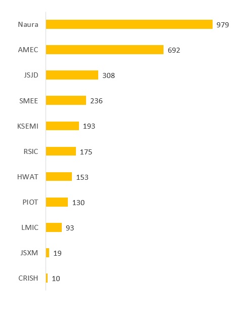
Naura is China's largest semiconductor equipment manufacturer, with its main products being etching and deposition devices. Its 2022 revenue reached US$979 million, significantly higher than AMEC, which was ranked second.

2022 revenue for China's main chipmaking equipment manufacturers (in million US$)

Source: Yole Intelligence, compiled by DIGITIMES, May 2023


Source: Yole Intelligence, compiled by DIGITIMES, May 2023

As with CXMT, although the company is not on the trade blacklist, the US export sanctions still posed significant challenges for the company's product roadmap realization. Right now, CXMT's 27nm memory density equivalent DDR4 and LPDDR4 have already hit the market. The third generation of products, equivalent to 1xnm, is also accelerating development. However, the existing roadmap may also be severely slowed due to the export sanctions.

To break out of this difficult situation, CXMT is actively chasing all kinds of necessary resources. Previous media reports pointed out that besides seeking an exemption from the export restrictions, CXMT was also pushing for an IPO at the Shanghai Stock Exchange STAR Market to obtain the funds required to expand its capital expenditures.

For now, the future of China's memory industry remains uncertain and the ongoing efforts of YMTC and CXMT may face even tougher challenges with the US government further tightening the trade restrictions. However, given that memory is a strategic focus of China's semiconductor ecosystem, it's expected that the local government and manufacturer will try everything they can to maintain the survival and operation of YMTC and CXMT.

Please, Log in or Register to view URLs content!
 

ansy1968

Brigadier
Registered Member
General agreement. But I am pointing out that there are things that China could do and haven't because of exactly what you are saying.

This whole idea that the US could afford things and China can't is more of a China don't want to.

A targeted security ban on rare earths to the US or Japan would create immediate stoppage and chaos sectorwide.
The American thinking is IF we sanction the Chinese since they were Asian like the Japanese they will do crazy things and launch a surprises attack like that of Pearl Harbor. So they can justify their aggression with the whole American public in support. The timetable is 2025, where the Arizona FAB will be in operational, they want a repeat of WW2 their ideal war and become the Arsenal of Democracy once again.

BUT the Chinese isn't biting cause they weren't ready and time is on their side especially with Russia providing the necessary natural resource that China needs, sorry for deviating now back to regular programming. ;)
 

Michaelsinodef

Senior Member
Registered Member
Big bans like Rare Earths should only really be done if actual conflict happens between China and the US, or the US goes full on economic warfare (kinda like what they have done to Russia), although the latter basically means China has no reason to trade stuff for USD, so it would be a big blanket ban on all things lol.
 

gelgoog

Lieutenant General
Registered Member
China should just either straight out ban exports of rare earths, or heavily tax them, they should only export magnets, etc. Manufactured products not the minerals.
 

tphuang

Lieutenant General
Staff member
Super Moderator
VIP Professional
Registered Member
Alright, I must warn everyone again to stop discussing banning rare earth, since it's off topic. There are many counter sanction methods which are possible, why is everyone only able to think of rare earths?

This is a semiconductor thread, please keep your suggestion to be semiconductor.
 

gelgoog

Lieutenant General
Registered Member
It is pretty obvious that China can do symmetric counter sanctions like they did with the Micron memory chips. The Chinese government can basically tell government owned companies not to buy Apple, Cisco, or other US products. In an extreme case they can also ban the sales of those companies in the whole Chinese consumer market.

I have been suggesting the Micron ban for like two years at this point, so it is about time they did it. Had China banned Micron two years ago when the US banned tool sales to JHICC perhaps the YMTC and CXMT tool bans would have never happened.

Unfortunately the more China remains passive the more the US thinks they can just walkover Chinese economic interests.
 

tokenanalyst

Brigadier
Registered Member

Kaixin Semiconductor received investment and is a supplier of core components for epitaxy equipment​


Recently, Suzhou Kaixin Semiconductor Technology Co., Ltd. (hereinafter referred to as "Kaixin Semiconductor") has received a new round of investment. Investors include Qianrong Yuanfeng Fund under Qianrong Holdings, Rockchip Investment, Bangming Longtou, Peking University Yuanpei Fund, Park Science and Technology Innovation Fund, etc.

It is reported that Kaixin Semiconductor focuses on the R&D, manufacturing and service of silicon carbide ceramic parts for semiconductor equipment. It has CVD core technology with completely independent intellectual property rights. Benchmark customers in other fields to achieve mass production supply.

The core product of Kaixin Semiconductor is the overall solution of CVD silicon carbide graphite base and thermal field of semiconductor epitaxy equipment, which belongs to the core components of semiconductor epitaxy equipment. In addition, the company also has rich technical reserves in the field of high-end ceramic components such as sintered silicon carbide ceramics and bulk silicon carbide ceramics.

In May 2022, Suzhou Industrial Park held a centralized signing event for key projects, and the Kaixin Semiconductor Materials R&D and Operation Headquarters project was among them.

Please, Log in or Register to view URLs content!
 

tokenanalyst

Brigadier
Registered Member
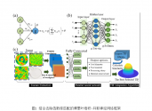
Shanghai Institute of Optics and Mechanics has made progress in adaptive process decision-making for ultra-precision optical surfaces based on supervised learning

Recently, the Precision Optical Manufacturing and Testing Center of Shanghai Institute of Optics and Fine Mechanics, Chinese Academy of Sciences has made important progress in adaptive process decision-making for ultra-precision optical surfaces based on supervised learning. The research team proposed a Fourier convolution-parallel neural network framework for the first time, which overcomes the bottleneck problem of high-dimensional output under the condition of small sample training in the field of optical processing, and the comprehensive training accuracy rate is better than 90%, realizing digital sub-aperture manufacturing The intelligent decision-making of multi-dimensional parameter combination processing has important guiding significance for the intelligent development of optical manufacturing. The relevant research results were published on Optics Letters under the title of "Fourier convolution-parallel neural network framework with library matching for multi-tool processing decision-making in optical fabrication" .

Modern optical systems such as photolithography systems, large telescopes and high-power lasers have put forward higher requirements for the quantity and surface quality of various ultra-precision optical components, while the existing process decisions still largely rely on experienced technical experts, Affected by the scarcity of professionals and the instability of manual decision-making, the intelligent decision-making process is a key issue for further improving the accuracy and efficiency of optical manufacturing. In recent years, the development of data-driven machine learning networks has made it possible to solve this bottleneck problem; however, in the field of optical processing, it is difficult to obtain training samples and the decision-making dimension is high. How to achieve effective training under small sample conditions to meet high feature dimension output Requirements are the primary problem facing the development of data-driven intelligent optical processing.

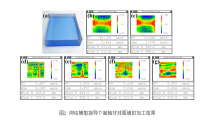
In response to the above problems, the research team proposed for the first time a Fourier convolution-parallel neural network framework combined with removal function library matching, which realized the joint autonomy of key parameters such as tool type, size, abrasive type and volume removal rate driven by data. Decision-making, the scope of decision-making covers most of the process flow from grinding/rough polishing to modifying/smoothing, and it is also the first time to prove the feasibility of optical manufacturing through data-driven neural network solutions. The experimental results show that only under the guidance of the network model, the surface precision (PV) of the 260mm260mm off-axis aspheric mirror can be converged from the initial 15.153λ to 0.42λ (λ=632.8nm), and the RMS can be converged from the initial 2.944λ to 0.064 λ, the total processing time is only 25.34 hours, and the convergence rate is better than 97%, which has reached the decision-making level of professional technicians. The research results are of great value to the efficient manufacturing of ultra-precision optical components, and may push the intelligent level of optical manufacturing to a new level.

1685106802510.png1685106827808.png

Please, Log in or Register to view URLs content!
 

ZeEa5KPul

Colonel
Registered Member
深蓝:Is the NA of the SMEE immersion lithography machine lens also 1.35?
havok: Yes
This is excellent. This moves SMEE to the state of the art in immersion DUV optics. The most capable ASML immersion DUV machines have this NA and it's very close to the theoretical (unattainable) maximum of 1.44. This is crucial in attaining a domestic 5/7nm node capability and particularly important since SMEE's production capacity is so limited. Every machine it makes must count.

I'd like to summarize what I've gathered about the state of China's EUV project. I'll consider the mechanical side of things since I know jack diddly about the chemistry (photomasks, photoresists, and so forth). I welcome corrections and elaborations from more knowledgeable members.

Light Source​

As I see it, there are two and a half EUV light source projects in China: SSMB, which China seems to be pursuing alone, and LPP, the mainstream approach in which China is experimenting with several arrangements (hence the "and a half").

SSMB: This seems to be the most promising long term solution to commercial EUV light sources and success here would allow China to leapfrog market leaders. However, what I gathered from reading research papers about this is that the challenges are significant. The operating parameters of the envisioned synchrotron are difficult: a 1A current and microbunch spacing of 3nm. For context, there is no synchrotron in the world that operates at 1A; the highest I've seen is 0.5A and the SSRF operates at 0.3A. However, it's plausible that since these are research synchrotrons that have to support a broad range of experiments, it might be easier to optimize a narrower set of parameters to a higher level in an industrial synchrotron. For the microbunch spacing, there's no comparable parameter in any other synchrotron so I have no context to point to, but the precision here seems exacting. SSMB is still in very early stages with a synchrotron being built in Xiong'an New Area, so it's unlikely to be part of China's first EUVL device.

LPP: This has the benefit of an existing proof of principle. We hear rumours that this is in the prototype stage, but things are understandably shrouded in secrecy. This is probably the most developed of the approaches China is trying and is likely to be first to market. Even here China is experimenting with several laser mechanisms. The first, and probably most explored, is a high-power (tens of kW) CO2 MOPA laser; this is the approach ASML uses. We've seen research that alternatives like "fiber lasers" are being explored. This can mean one of two things:

1) A genuine solid-state fiber laser where the gain medium is a fiber optic doped with a rare-earth element. Although both CO2 and fiber lasers emit in the infrared, fiber lasers emit wavelengths between 1-2um (depending on the dopant), while CO2 lasers emit at 10.6um. This will almost certainly have implications in the interaction of the laser with the tin droplets. However, it would be great news if it's workable since China has a great deal of experience with high-power fiber lasers. I've joked previously that Norinco should take a Silent Hunter and point its laser at a tin droplet assembly.

2) A "hollow fiber" laser in which the fiber is just a transmission medium rather than the gain medium. In this arrangement, rather than have a monolithic CO2 MOPA laser, the output of several smaller CO2 MOPA lasers can be combined using hollow fibers. Classical fiber optics aren't usable here since glass absorbs 10.6um IR. Needless to say, this would be promising because smaller, lower-power modular lasers are easier and cheaper to build than giant, monolithic, high-power lasers.

Optics and Wafer Stage​

There's some great news here. EUV light is one of the most troublesome parts of the spectrum to deal with. The light is very difficult to generate and everything absorbs it. Water, air, silica, everything. Given this property, refractive optics like those used in DUV lithography are impossible. All optics have to be reflective (i.e., some type of curved mirror). In this particular case, mirrors are fabricated using alternating layers of molybdenum and silicon. To overcome this challenge, China needs to be good at manufacturing and polishing large, curved mirrors to very high precision.

Wait, what's that? Oh look, it's our old friends at CIOMP:
Please, Log in or Register to view URLs content!


(Note: Large Si/Mo aspheric mirrors have the added challenge beyond grinding and polishing the substrate in that precise control of Si/Mo layer deposition is required.)

There's not much to say about the wafer stage. We've already heard from havok that there's a prototype vacuum maglev dual-stage workpiece with multi-axis laser interferometer and all the fixin's you please.

It's all coming together!
 
Last edited:
Status
Not open for further replies.
Top