Chinese semiconductor industry

Status
Not open for further replies.

tokenanalyst

Brigadier
Registered Member

Honghu Semiconductor completed the A+ round of strategic equity financing and is committed to the localization of wafer transfer equipment​


Recently, Honghu (Suzhou) Semiconductor Technology Co., Ltd. (hereinafter referred to as "Honghu Semiconductor"), as a leading supplier of semiconductor wafer transfer equipment in the industry, has completed hundreds of millions of yuan in A+ round of strategic equity financing. Investment Ventures led the investment, Shenzhen High-tech Investment, Yuanhe Yuandian, Zhidao Capital, Yongxin Ark and other joint investments, and the old shareholder TEDA Technology Investment continued to invest. The funds raised in this round of financing will be used to accelerate product research and development, expand the scale of operations, strengthen the development and layout of international and domestic sales markets, etc., to consolidate and continuously improve the comprehensive competitiveness of Honghu Semiconductor in the field of global semiconductor equipment components.

Honghu Semiconductor was established in Suzhou. It is a national high-tech enterprise specializing in the R&D and manufacturing of semiconductor wafer transfer automation equipment, and is committed to the localization of wafer transfer equipment and core components. The main products include equipment front-end modules (EFEM), wafer Film transfer machine (Sorter), vacuum transfer platform (VTM), semiconductor core precision transfer components, etc. For a long time, Honghu Semiconductor has been based on independent research and development, and wafer transfer equipment has been used in the front, middle and back-end processes of semiconductor equipment.

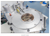
1684841434611.png1684841477122.png

Please, Log in or Register to view URLs content!
 

tphuang

Lieutenant General
Staff member
Super Moderator
VIP Professional
Registered Member
I actually don't see requiring licenses on Nikon DUVi scanners will affect China all that much. I agree with the sentiment that this is done with pressuring Dutch gov't in mind. If Chinese fabs are not fast tracking orders through, then they are just being stupid.

The other item to note is how will this get implemented. If it gets implemented where only new orders require licenses or where there is a grace period. That's quite different from the hard stop that the October surprise required. I think it's important to over react until we get more details
 

zbb

Junior Member
Registered Member
I predict Japan may institute requiring licenses for wide range of semi exports but then follow the US lead of approving all the license applications. US approves 94% of licenses to export to China.

Please, Log in or Register to view URLs content!

Because if even US approves nearly all tech export to China that requires licenses, Japan will have their own Potemkin village of export controls and then follow in same footsteps. The implementation is the key, and so far it's not even fully enforced by US.
The high 94% approval rate for US export licenses is very misleading.

When export licenses are denied, the prospective buyers and sellers will know that future export license applications will also be denied and won't bother going through the expense of applying for such licenses again.

On the other hand, when export licenses are approved, the buyers and sellers will very likely be applying for many more export licenses for similar transactions in the future.

The end result of the above dynamics is that the export license approval rate will always be very high regardless of how restrictive the export licensing rules are.
 

tokenanalyst

Brigadier
Registered Member

The first phase project of the industrialization of electronic information materials and devices in Jingzhou Pioneer, Hubei started​


It is reported that the project was built by Guangdong Leading Rare Materials Co., Ltd. with an investment of 20 billion yuan. The project will be constructed in two phases. The first phase will invest 6.5 billion yuan and cover an area of 1,352 mu. It plans to build electronic information special materials and rare metal resource recovery projects. At the same time, it will construct public and auxiliary facilities such as sewage treatment and power base stations. It is expected to be completed by the end of 2024. officially put into production.
According to the official website of Xiandao Rare Materials, Xiandao Company started to set foot in the rare metal industry in 1995, and officially changed its name to Xiandao Rare Materials in Qingyuan in 2003. A high-tech enterprise with R&D, production, sales and recycling services, it has a national rare metal engineering technology research center, a nationally recognized enterprise technology center, a post-doctoral research workstation, and an independent advanced materials research institute.
A few days ago, a major project in Jiangsu Province in 2022-Xuzhou Leading Semiconductor Thin Film Material Project has made new progress, and it is expected to have production capacity early next year. It is reported that the total investment of the project is 6.7 billion yuan, and it mainly produces semiconductor thin film materials. After reaching full capacity, it can realize an annual output of about 100 tons of semiconductor targets, about 50,000 meters of bonding wire, about 200 tons of microelectronic targets, and rare metal powders. About 300 tons, about 1 million pieces of substrate materials.​
 

european_guy

Junior Member
Registered Member
Nanda Optoelectronics: The company's ArF photoresistor products have passed the verification of memory chips and logic chip manufacturers
Please, Log in or Register to view URLs content!

They said the same thing 2 years ago.

The problem with Nata is that for some reason they cannot produce in volume.....nothing has changed in this regard.
 

tokenanalyst

Brigadier
Registered Member

Penumbra Optical Lithography Reticle and Micro-nano Optical Devices Project Signed in Nantong​

On April 21, Penumbra Optics (Nanjing) Co., Ltd. signed an investment agreement with Jiangsu Nantong Haimen Development Zone to plan and construct micro-nano optical devices and semiconductor photomask production projects with a total investment of 500 million yuan.
According to news from Haimen Development Zone, Penumbra Optics (Nanjing) Co., Ltd. is mainly committed to the design, production and service of diffraction components, CGH, gratings, photomasks and other products. The photomask products produced by the company have made technological breakthroughs. The path of traditional nanoimprinting to produce optical devices simplifies the process flow, and it is also the only company in China that has mastered the use of semiconductor technology for mass production of pure quartz structured optical products.
According to the news from Tianyancha, Penumbra Optics was established on October 29, 2020, with a registered capital of 863,158 yuan, and has received multiple rounds of financing. Investors include Yida Capital and others.

Please, Log in or Register to view URLs content!
 
Status
Not open for further replies.
Top