Chinese semiconductor industry

Status
Not open for further replies.

tokenanalyst

Brigadier
Registered Member
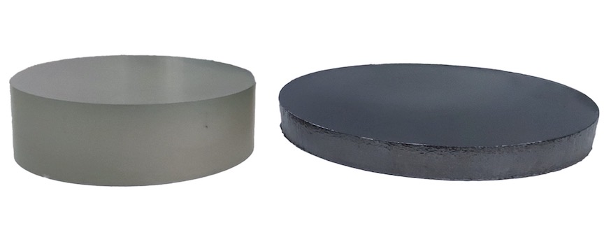
AMEC is expanding into all areas of semiconductor production, not just logic, DRAM, etc. this means that they're doing analog, power, RF, LED, etc. I also believe in this paper, they're demoing their MOCVD production tools, which is something new as they're best known for etching.

Please, Log in or Register to view URLs content!

Its a short step from MOCVD to ALD. That means AMEC is rapidly expanding its technical offering and becoming more like NAURA, rather than only etch focused semiconductor company. There's many 1 sector companies, but much harder to become something like LAM, AMAT or TEL.
I think also point out the modern collaborative approach between the Chinese semiconductor industry and research institutions in designing the manufacturing process of different devices, that means that Chinese equipment is probably going to become the standard for the manufacturing of these devices in the future.​
This kind of industry-academy collaboration was less common in the past and more common today. US companies benefited from this approach as semiconductor fab companies collaborated with Chinese academia and US toolmakers to design their process around US tools, that is why when US companies pull out was bad because a lot of the process where designed around US made tools.

1683403604841.png
So in the future is probably that we are going to see less or any collaboration in process design with US tool companies and more collaboration with Chinese tool companies

Please, Log in or Register to view URLs content!
 
Last edited:

tphuang

Lieutenant General
Staff member
Super Moderator
VIP Professional
Registered Member
I do remember reading in amec's year end report that they have been getting into micro led. I just never heard of this duv led. Are you saying this is going to be the next type of screen that becomes big? I don't know why other countries would necessarily adapt to Chinese standards in production of duv led @tokenanalyst and @FairAndUnbiased
 

FairAndUnbiased

Brigadier
Registered Member
I do remember reading in amec's year end report that they have been getting into micro led. I just never heard of this duv led. Are you saying this is going to be the next type of screen that becomes big? I don't know why other countries would necessarily adapt to Chinese standards in production of duv led @tokenanalyst and @FairAndUnbiased
DUV LED isn't for screens. It would be very bad for humans to look at DUV, as it is both chemically active to organic molecules such as that found in eyes, and you can't see it. An invisible screen that burns your eyes out is unlikely to be welcomed by consumer markets.

DUV LEDs are for industrial UV light sources which are currently being produced by extremely expensive tools. Previously, 365 nm i-line Hg lamps were used. Now for most applications (including some forms of lithography) they are getting replaced by 365 nm LEDs.

Imagine KrF excimer sources costing 500k being replaced by a 5k LED source. Cabbagization of KrF lithography down to 90 nm? Maybe, maybe not, but it's at least a physical possibility now.
 

ZeEa5KPul

Colonel
Registered Member
DUV LED isn't for screens. It would be very bad for humans to look at DUV, as it is both chemically active to organic molecules such as that found in eyes, and you can't see it. An invisible screen that burns your eyes out is unlikely to be welcomed by consumer markets.

DUV LEDs are for industrial UV light sources which are currently being produced by extremely expensive tools. Previously, 365 nm i-line Hg lamps were used. Now for most applications (including some forms of lithography) they are getting replaced by 365 nm LEDs.

Imagine KrF excimer sources costing 500k being replaced by a 5k LED source. Cabbagization of KrF lithography down to 90 nm? Maybe, maybe not, but it's at least a physical possibility now.
That's amazing! Can the physical principles behind those LEDs be pushed down to 193nm?
 

tokenanalyst

Brigadier
Registered Member

Six-inch conductive crystal ingot and four and a half inch insulating crystal ingot​


4-inch semi-insulating silicon carbide crystal, micropipe density <0.5cm -2 , resistivity > 10 6 Ω·cm, no obvious cracks, inclusions, polymorphic defects, etc. The product meets the industry standard and is at the leading level in the industry .

The density of 6-inch conductive silicon carbide micropipes is <0.1cm -2 , the total dislocation density is <8000cm -2 , the resistivity is 0.015~0.025Ω·cm, and there are no obvious defects such as cracks, inclusions, and polytypes. level standard, at the leading level in the industry.

20220331115342_6029.jpg


Laser lift-off technology​


Dry Crystal Semiconductor (ivsemitec) has developed a new type of slicing technology, which is expected to solve the problem of large material loss during silicon carbide processing. The process route is shown in the figure below. The core of laser lift-off technology is to use laser pulses to form an amorphized layer of silicon carbide at a preset depth inside the ingot, and then use external force to separate the wafer from the amorphized layer, thereby obtaining a wafer with a target thickness. The method of obtaining wafers by laser lift-off has low material loss during processing, the thickness of the defect layer on the wafer surface is small, and the total material loss rate can be reduced to about 20%, which is expected to greatly reduce the cost of wafers. Compared with multi-wire cutting, laser processing produces no waste liquid and is more environmentally friendly. Laser processing is not limited by the hardness of the material, and has good processing efficiency for superhard materials.

20220317102549_2348.png


This technology can not only be applied in the field of silicon carbide slicing, but also has application prospects for the reuse of silicon carbide and gallium nitride substrates after device processing, which can reduce the unit cost of devices on expensive substrates. At present, the team is optimizing the laser processing technology and stripping technology, and is seeking industrial cooperation for this technology.


20220317103300_9436.png


Please, Log in or Register to view URLs content!
 

FairAndUnbiased

Brigadier
Registered Member
That's amazing! Can the physical principles behind those LEDs be pushed down to 193nm?
I am not sure.

In a LED, the energy of the photon emitted is equal to the bandgap energy of a semiconductor. Just like how a ground state atom can have an electron excited up into an unoccupied orbital, so can solids. What happens when an excited state electron falls back down into the ground state? The energy difference is released as light. Analogously, the same happens for LEDs, except instead of for individual atoms, it is for a huge number of atoms in a solid at once.

254 nm for KrF is 4.8 eV. 193 nm is 6.4 eV. Many common semiconductor materials have >5 eV bandgap. In the paper they use AlGaN, since AlN has a 6 eV bandgap and III-V compound semiconductors have the property of being able to tune their bandgap by alloying with other Group III metals like Ga, In, etc.

However, pure AlN with a 6 eV bandgap cannot be used as a semiconductor, as the high bandgap means not enough charge carriers at room (or even very high) temperature. It must be doped with a carrier donor to increase conductivity.

Please, Log in or Register to view URLs content!

As bandgap gets higher the more difficult (higher voltage required) to push current through the material and the less efficient the process is due to high heat generation. In addition the bandgap of the material is related to the crystal structure and thus temperature, so the bandgap can shift if there's poor cooling. Meanwhile light atomic sources like ArF or KrF excimer lamps don't have much temperature dependence.

Commercially available LEDs go down to 215 nm but they're used for analytical sources that are small.

Please, Log in or Register to view URLs content!

KrF lamps already are at 8.7% efficiency. So a DUV LED must exceed this to be used for lithography (but not for anything else that requiers 254 nm or large area exposure like photochemical machining)

Please, Log in or Register to view URLs content!
 

latenlazy

Brigadier
I am not sure.

In a LED, the energy of the photon emitted is equal to the bandgap energy of a semiconductor. Just like how a ground state atom can have an electron excited up into an unoccupied orbital, so can solids. What happens when an excited state electron falls back down into the ground state? The energy difference is released as light. Analogously, the same happens for LEDs, except instead of for individual atoms, it is for a huge number of atoms in a solid at once.

254 nm for KrF is 4.8 eV. 193 nm is 6.4 eV. Many common semiconductor materials have >5 eV bandgap. In the paper they use AlGaN, since AlN has a 6 eV bandgap and III-V compound semiconductors have the property of being able to tune their bandgap by alloying with other Group III metals like Ga, In, etc.

However, pure AlN with a 6 eV bandgap cannot be used as a semiconductor, as the high bandgap means not enough charge carriers at room (or even very high) temperature. It must be doped with a carrier donor to increase conductivity.

Please, Log in or Register to view URLs content!

As bandgap gets higher the more difficult (higher voltage required) to push current through the material and the less efficient the process is due to high heat generation. In addition the bandgap of the material is related to the crystal structure and thus temperature, so the bandgap can shift if there's poor cooling. Meanwhile light atomic sources like ArF or KrF excimer lamps don't have much temperature dependence.

Commercially available LEDs go down to 215 nm but they're used for analytical sources that are small.

Please, Log in or Register to view URLs content!

KrF lamps already are at 8.7% efficiency. So a DUV LED must exceed this to be used for lithography (but not for anything else that requiers 254 nm or large area exposure like photochemical machining)

Please, Log in or Register to view URLs content!
Also need to keep in mind material breakdown from constant high voltage cycling. Even if you could get a material to emit at 193 um you might have short lifetime from burnout. These are all sorts of material chemistry problems that may take a lot of time and effort to resolve for commercial application.
 

tphuang

Lieutenant General
Staff member
Super Moderator
VIP Professional
Registered Member
According to Dylan Patel, big layoffs coming at Intel

so for biggest losers of US/China trade wars, we have
Boeing, Intel, Micron

and presumably
Amat, Lam & KLA will see huge drops soon.
It would seem to me that TI and Onsemi would be in China, but that hasn't really played out yet.
 

tphuang

Lieutenant General
Staff member
Super Moderator
VIP Professional
Registered Member
Screen Shot 2023-05-07 at 8.23.27 AM.png
For all the Huawei fanboys, great news if true from Hisilicon guy

there will not be a whole new Kirin SoC this year
best case to achieve 5G in a Huawei phone is to also have a Balong chipset on the phone (Huawei whisper says no 5G on Mate 60 on another post)

We will see Kunpeng-930 and Ascend-920 to be released later this year

Again, it seems like Huawei has prioritized Kunpeng CPU, Ascend GPU, Tiangang base station chip & auto SoC ahead of smartphone. That makes sense given the # of chips needed for smartphones and their lack of competitiveness vs high end QCOM SoC

Anyways, I hold out hope that Kunpeng-930 and Ascend-920 will both prove to be vastly improved over Kunpeng-920 and Ascend-910 through advanced packaging & improved design. After all, Biren managed to achieve 1000 TFLOPS on FP16 with 7nm TSMC process. No reason Ascend GPUs can't have significantly higher computation power than it does now
 

Wahid145

New Member
Registered Member
According to Dylan Patel, big layoffs coming at Intel

so for biggest losers of US/China trade wars, we have
Boeing, Intel, Micron

and presumably
Amat, Lam & KLA will see huge drops soon.
It would seem to me that TI and Onsemi would be in China, but that hasn't really played out yet.
Really wanna see AMAT LAM and KLA go down like Motorola, Compaq and other very well known american brands which got reduced to dirt
 
Status
Not open for further replies.
Top