Chinese semiconductor industry

Status
Not open for further replies.

tokenanalyst

Brigadier
Registered Member
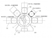
Interesting hybrid PVD-RTA, PVD-rapid thermal annealing tool for MEMS fabrication being develop by this company.

1683218258087.png
1683218368898.png

Zhejiang Aiweipu Technology Co., Ltd. was founded in Haining, Zhejiang by a team of entrepreneurs who have returned from Silicon Valley and a team of entrepreneurs in cooperation with Haining Tiantong Group. The company has gathered a number of senior semiconductor equipment, process and material experts at home and abroad, focusing on building world-leading high-end semiconductor and new energy equipment.
The company's core technologies and products include PVD, IBE, RIE and other series of semiconductor, MEMS, new energy device manufacturing equipment. With professional advantages and excellent services in Silicon Valley, the company has won international reputation. Its products are widely used in semiconductor, hard disk, MEMS and other industries. Strategic suppliers, partners.
The company is headquartered in Zhejiang Haining Pan-Semiconductor Industrial Park, covering an area of nearly 6,000 square meters, with more than 1,000 square meters of 1,000-class ultra-clean rooms.

some of their tools

1683218451884.png

Please, Log in or Register to view URLs content!
 

HighGround

Senior Member
Registered Member
We essentially ask the fabs to take 15 to 20% margin hits in order to help domestic industry. There is a reason why domestic equipment really took off after October. Commercial companies have to stay afloat first. They will always want to use tools that are the most economical to them. Using worse, more cumbersome tools hurt their ability to be competitive.

Isn't this true of any new tool?

It's not necessarily that the tool is bad, even if the tool was better it still takes time to train your workforce on how to use it and integrating it into existing work lines or creating new ones.
 

FairAndUnbiased

Brigadier
Registered Member
This is normal. The biggest problem in China's semiconductor manufacturing industry has never been technology, but the absence of a market. The semiconductor manufacturing industry has always been very closed. And SMIC has never wanted to use domestic equipment.
This is true. SMIC isn't a public sector enterprise, a cooperative (Huawei), a private enterprise run by those motivated by both profit and patriotism (Baidu) or even just for money (Alibaba).

Based on my understanding it used to be a Taiwanese style fab that's just physically in mainland China. They even have an on site Taiwanese private school teaching a US curriculum.

Please, Log in or Register to view URLs content!

Can't rely on them. It'll be nice if they help, but don't expect them to help much more than Foxconn.
 
Last edited:

tokenanalyst

Brigadier
Registered Member

720,000 pieces! The SiC project is about to go into production.​


Recently, the domestic silicon carbide project has made new progress. It is expected to be put into production in the fourth quarter of this year. After reaching the production capacity, it will form an annual production capacity of 720,000 power chips.

On April 25, the Nanhu District People's Government issued a document stating that in the first quarter of this year, investment in manufacturing and technological transformation in the region achieved a "good start", completing 2.518 billion yuan and 1.422 billion yuan respectively, with growth rates of 55% and 72.8% respectively.

According to reports, the R&D and industrialization projects of high-voltage characteristic process power chips and SiC chips built by STAR in Nanhu District, Jiaxing City, Zhejiang Province, currently two of its factories have started debugging equipment, and other factories are waiting for acceptance, which is expected to be completed in the fourth quarter of this year . It will be put into production and will form an annual production capacity of 720,000 power chips after reaching the production capacity.

Please, Log in or Register to view URLs content!
 

tphuang

Lieutenant General
Staff member
Super Moderator
VIP Professional
Registered Member
Please, Log in or Register to view URLs content!
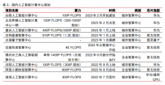
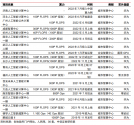
lol, I found the CITIC securities report summary of data centers since 2021 and whose GPUs they used. Aside from Tencent, Alibaba & Baidu, which most likely will never use Huawei GPUs, almost everyone else used Huawei GPUs. Which would confirm the viewpoint by many that Ascend GPUs are best AI chips in China in production for the past couple of years. I guess with Cambrian winning a couple of times. The part that Huawei won works out to be almost 8 EFLOPS
wqNG76ySv4.png
8WQs7CRtCD.png
ChatGPT 是大模型商业化落地的标杆,其底层模型GPT-3 共有1750 亿参数,训练所需算力和成本均高出传统NLP 模型,云算力资源训练成本估算约460 万美金。国内千亿参数大模型如华为盘古使用超过2000 块华为昇腾910 以640PFLOPS 的FP16 算力训练超过两个多月,可见大模型训练算力耗费之巨大,算力扩容需求明确。
2000 Ascend 910 GPU produces 640PFLOPS of FP16 computation need 2+ months, so each is 320 TFLOPS of FP16

Considering that A100 supports 300 TFLOPS, it really backs up the theory that Ascend-910 for the past couple of years was the closest China had to A100.

拓维信息为华为昇腾核心合作伙伴,2022H1 昇腾硬件出货量第一。拓维信息是首批昇腾授权的人工智能计算硬件生产合作伙伴,其AI 训练服务器可搭载8 张昇腾910,提供2.56P FLOPS 的FP16 算力,目前已应用于长沙人工智能创新中心、重庆人工智能创新中心、全国一体化算力网络国家(贵州)主枢纽中心等项目中。据公司披露,2022 年上半年,拓维信息昇腾计算硬件出货量位列华为昇腾合作伙伴排名第一。
Again 8x Ascend 910 is 2.56 PFLOPS of FP16 computation. Used in Changsha & Chongqing

各城市处设与规划人工智能计翼中心的意原强烈,华为盘古大模型需要64PFLOPS的算力来支持运夏,据
Please, Log in or Register to view URLs content!
测算,以资源共享以及优化配置的角度来看,假设未来部分企业大模型训陈需要租用公共算力设施,且因为目前华为方案为主流,所以算力标准相同为FP16现有城市人工智能算力中心算力(100P-300PFLOPS)仍有数倍提升空间。以北京为例,北京规划短期算力规极提升至500PFLOPS,远期达到1000PFLOPS,以舞腾910卡为例若想从100PFLOPS提到500PFLOPS标准,则需要八卡服务器156个
For example, if beijing was to expand from 100 to 500 FLOPS, would need 156 AI training servers of 8x Ascend-910 GPU
Please, Log in or Register to view URLs content!
:

公司是华为的核心战略合作伙伴,包括界腾生态的合作。公司与华为的合作覆盖华为的多个产品线和服务领域。公司发布了神州鳃泰人工智能推理服务器,以“鳃鹏+界腾”为核心,可提供128个处理核心的算力。目前公司已累计为超过300家中大型企业提供云服务《其中世界五百强客户超50家),紧计迁移超过1.5万台云服务器,管理超过1万台云服务器。
Also has this company that's core partner of Huawei which build intelligent server machines using Kunepng + Huawei chips to provide 128 core computation (so maybe 2x64 core Kunpeng-920 with 8 Ascend 910). Already migrated over 15000 of such cloud server and manage over 10000 such server. So looks like they've sold a lot of these GPUs and have large contracts to expand enough more. This part is not for smart city but rather just medium large enterprises.
 

sunnymaxi

Captain
Registered Member
Please, Log in or Register to view URLs content!

China’s TanKeBlue to Supply SiC Wafers, Boules to German Chip Giant Infineon


Chinese silicon carbide supplier TanKeBlue Semiconductor has penned a long-term contract to supply SiC wafers and boules to Infineon Technologies, Germany’s largest chipmaker.

TanKeBlue will provide 150 millimeter SiC wafers and boules to Infineon to manufacture SiC semiconductors in the initial phase, covering a double-digit share of expected long-term demand, the Neubiberg-based firm said in a press release yesterday. It will also supply 200 mm SiC material to support Infineon's transition to 200 mm wafer diameter, it added.

The agreement will diversify Infineon's SiC supplier base, according to the company. It also contributes to general supply chain stability and growing demand for SiC chip products for auto, solar, and electric vehicle charging applications as well as energy storage systems in the Chinese market, it pointed out.

“Infineon is significantly expanding its manufacturing capacities at its production sites in Malaysia and Austria to meet the growing demand for SiC,” said Chief Procurement Officer Angelique van der Burg. “In order to offer the most comprehensive product range possible to our customers, Infineon is currently doubling down on its investments in SiC technology and product portfolio.”

Infineon is implementing a multi-supplier and multi-country sourcing strategy to increase resilience to benefit its broad customer base, van der Burg noted.

To hit its target of a 30 percent global market share by the end of this decade, Infineon's SiC manufacturing capacity will increase 10-fold by 2027, the press release said.
 

gelgoog

Lieutenant General
Registered Member
SMIC founder Zhang Rujing had been looking towards making a fab in China for quite a long time. If all he wanted was a steady job, he could have just continued working at TSMC. Even after he was dismissed from SMIC, he has continued to help bootstrap various foundries in mainland China including SiEn.

After he left, most of the C-suite personnel at SMIC are mainland Chinese. While there are a lot of Chinese from Taiwan at SMIC, they are not in control of the company. The company did start out with international capital, but it has long moved over to Chinese capital.
 

tokenanalyst

Brigadier
Registered Member
School of Electronics develops two-dimensional transistor with speed exceeding silicon limit


Chips provide a steady stream of power for the development of big data and artificial intelligence. The increase in chip speed is due to the miniaturization of transistors. However, the performance of traditional silicon-based field-effect transistors is gradually approaching its intrinsic physical limit. The International Roadmap for Devices and Systems (IRDS) predicts that the limit gate length of silicon-based transistors will stop at 12 nm, and the operating voltage cannot be less than 0.6 V, which defines the end of the silicon-based chip scaling process in the future Therefore, it is urgent to develop new channel materials to continue Moore's Law. Atomic-thick two-dimensional semiconductors have attracted widespread interest from both the scientific and industrial communities as one of the strong candidates for future chip channel materials due to their ultrathin body and high mobility. In recent years, the world's leading semiconductor manufacturing companies and research institutions such as Intel, TSMC, Samsung and the European Microelectronics Center have invested in research on 2D materials. However, limited by the bottlenecks of contacts, gate dielectrics, and materials, the performance of all two-dimensional transistors so far cannot match the industry's advanced silicon-based transistors, and the experimental results are far behind theoretical predictions, which are not enough to demonstrate the potential of two-dimensional semiconductors. ultimate potential.
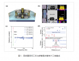
Recently, the research team of Professor Peng Lianmao and Researcher Qiu Chenguang from the School of Electronics, Peking University has prepared a 10nm ultra-short channel ballistic two-dimensional indium selenide transistor, which for the first time made the actual performance of exceed that of Intel's commercial 10nm node silicon - based fin. Transistor, and the working voltage of the two-dimensional transistor is reduced to 0.5 V , which is also the fastest and lowest power consumption two-dimensional semiconductor transistor in the world so far . The relevant research results are titled "Ballistic two-dimensional InSe transistors", published online in Nature on March 22, 2023, web link:
Please, Log in or Register to view URLs content!
-w#citeas
). Doctoral students Jiang Jianfeng and Dr. Xu Lin from the School of Electronics are the co-first authors, Professor Peng Lianmao and researcher Qiu Chenguang are the co-corresponding authors, and the School of Electronics of Peking University is the sole unit of the paper.
This work has achieved three technological innovations: using three layers of indium selenide with high carrier thermal velocity (smaller effective mass) as the channel, and achieving a room temperature ballistic rate as high as 83%, which is the highest value of field effect transistors at present. Much higher than the ballistic rate of silicon-based transistors (less than 60%); solved the problem of growing ultra-thin oxide layers on the surface of two-dimensional materials, prepared 2.6 nanometer ultra-thin double-gate hafnium oxide, and increased the device transconductance to 6 mS Micron, an order of magnitude more than all two-dimensional devices; pioneered doping-induced two-dimensional phase transition technology to overcome the international problem of gold-half contacts in the field of two-dimensional devices, refresh the total resistance to 124 ohm microns, and meet the requirements of future nodes of integrated circuits for transistors Resistor requirements (220 ohms • microns).
Comparing with the development roadmap of silicon-based devices predicted by the industry’s IRDS, the ballistic two-dimensional indium selenide transistor realized by the Peking University team broke the four ultimate silicon-based “red walls”: 1) The trench length was reduced to 10 nanometers (beyond silicon-based limit of 12 nm), while maintaining an ideal subthreshold swing of 75 mV range, DIBL is only 20 mV/V, and the off-state characteristics of the device exceed the best silicon-based FinFET technology. 2) The voltage is scaled down to 0.5V (beyond the 2031 silicon-based limit of 0.6V), and the device current is turned on from the standard off-state of 100nA/micron to more than 1mA/micron on-state. 3) The gate delay is reduced to 0.32 picoseconds, which is four times better than the silicon-based limit of 1.26 picoseconds. 4) The power consumption delay product is reduced to 4.32E-29JS/micron, which is an order of magnitude lower than the silicon-based limit.

Please, Log in or Register to view URLs content!
 

tokenanalyst

Brigadier
Registered Member
Zhang Zhiyong's research group from the Carbon-Based Electronics Research Center has made important progress in the field of carbon nanotube monolithic 3D integrated circuits

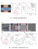
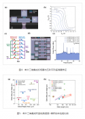
The pursuit of comprehensive performance of future integrated circuits for performance × power consumption × area (PPA) has made the manufacture of advanced silicon-based integrated circuits gradually slow down the limit reduction of technology nodes and physical dimensions, and instead develop the three-dimensional integration of vertical dimension transistors and circuits technology to seek breakthroughs. Compared with advanced three-dimensional packaging with a mature application market, monolithic three-dimensional integration technology is based on the manufacturing process of semiconductor front-end active transistors and back-end interconnection, which has higher interlayer interconnection density and transistor integration density, and theoretically has circuit synthesis. Higher potential for performance. In the field of silicon-based monolithic three-dimensional integration, due to the thermal tolerance of transistors, the fabrication temperature of the upper monocrystalline silicon channel and active transistors is forced to decrease, resulting in a large gap in the performance of the upper layer compared with silicon-based advanced technology nodes , there is still a certain bottleneck. The parallel array carbon nanotube material with high density and high semiconductor purity has low-temperature material preparation and transistor processing technology, and has a high level of thermal tolerance, which is conducive to monolithic three-dimensional integrated processing. Moreover, the monolithic three-dimensional integrated architecture reduces the interconnection length of carbon tube circuits, which is conducive to the improvement of circuit speed ( Nano Res . 2019;12(8):1810). Therefore, carbon nanotube transistors are very suitable for building high-speed monolithic three-dimensional integrated circuits. However, the field of monolithic 3D integration of carbon nanotubes still lacks high-quality interlayer processes and upper channel materials, which limits the performance of monolithic 3D integrated transistors and circuits.​

1683233401445.png1683233433347.png
1683233364520.png

Please, Log in or Register to view URLs content!
 
Status
Not open for further replies.
Top