Xi also cleansed CPC from CIA stooges, I remember Western propaganda media whining non-stop about it, so he was and is a visionary in that regard. I bet if it was solely dependent on Xi, he would have started semiconductor self-sufficiency push long ago but all the liberal cucks in the government and companies stalled the process until the US started sanctioning every single thing they could find. Even then, some idiots want to succumb instead of working on alternatives but they are now in the minority.Among his many quotes I remember where Chinese President Xi Jinping likened a microchip to the to the human heart, saying "no matter how big a person is, he or she can never be strong without a sound and strong heart"
Of course the "person" he refers to is China....it was in 2018!
You are using an out of date browser. It may not display this or other websites correctly.
You should upgrade or use an alternative browser.
You should upgrade or use an alternative browser.
Chinese semiconductor industry
- Thread starter Hendrik_2000
- Start date
- Status
- Not open for further replies.
Shengmei Shanghai: 18-cavity cleaning equipment products have completed client verification

According to news from Jiwei.com, recently, an investor asked a question on the investor interaction platform: Excuse me: How much is the general price range of the company's 16-cavity cleaning equipment?
Shengmei Shanghai (688082.SH) stated on the investor interaction platform on March 27 that the company's cleaning equipment products do not have 16 cavities, but 18 cavities and have completed client verification, mainly focusing on the memory market. The company does not publicly disclose the prices of specific products. Semiconductor special equipment products have significant customization features, and different customers may have different product configurations, performance requirements and bargaining power.
As of press time, the market value of Shengmei Shanghai is 39.194 billion yuan, and the stock price is 90.40 yuan per share, an increase of 0.67% from the closing price of the previous day.
Hunan Upgraded their E-Beam software to run in High Performance Parallel Computers.


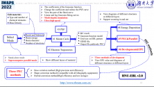
An EDA tool for e-beam lithography (EBL) developed at Hunan University (HNU)
View attachment 85770
The EBL-oriented EDA software tools are indispensable to design and manufacture EUV/DUV masks or sub-10 nm prototype devices. Some international treaties (e.g., 3.D.1-3 of Wassenaar Agreement [1]) and national laws (e.g., 3D003 of U.S. export control laws [2]) impose controls on exporting EBL-oriented EDA software tools to certain countries like China, Russian, etc.
We believe that EBL technologies should be used as friendly tools to improve lives of people from all countries without discrimination, rather than hostile weapons to deter the development of any country. Therefore, we are trying to develop these EBL EDA tools from scratch by ourselves. We license HNU-EBL EDA software, free of charge, to anybody from anywhere. To obtain a license, please click “license” and “contact us” on the top.
If that is not a giant middle finger, i don't know what else it is.


A Plasma Etch Method for CircularTruncated Cone Through Silicon Via for Advanced Packaging
LIN Yuanwei, ZHAO Jinrong, CAO Zejing, YUAN Renzhi- Department of Semiconductor Etching, NAURA Technology Group Co.,Ltd., Beijing 100176, China
Abstract: It becomes more and more difficult to maintain Moore's law in the manufacturing stage of integrated circuits, and the use of three-dimensional space in the packaging stage can be regarded as an extension of Moore's law. Silicon via is a common technology to realize advanced packaging by using three-dimensional space. In the existing technology, the circular truncated cone through silicon via applied to the packaging of CMOS image sensor devices is realized by continuous transverse etching on the top, which is hard to improve the packaging density and has certain requirements for the resolution of lithography equipment. Aiming at the problems in the existing technology, a circular truncated cone through silicon via hole with strict controlled transverse etching (undercut size is 3%-12% of the critical dimension) has been studied and explored. By adjusting the power of the lower electrode (not more than 30 W is required), this method can obtain a circular truncated cone through silicon via hole with adjustable side wall angle (70°-88°) and the size of the through-hole bottom opening smaller than the defined characteristic size of lithography. This method is expected to be extended to three-dimensional integrated circuits, which will help to maintain Moore's law in the packaging stage.

They also using SMEE SSB500 for this process.
Shengmei Shanghai won the first purchase order for Ultra C SiC silicon carbide substrate cleaning equipment
Supports fast-growing power semiconductor markets, including electric vehicles, power conversion and renewable energy
Shengmei Semiconductor Equipment (Shanghai) Co., Ltd. (hereinafter referred to as "Shengmei Shanghai") (Science and Technology Innovation Board stock code: 688082), as a leading provider of wafer process solutions for semiconductor front-end and advanced wafer-level packaging applications supplier, today announced its first purchase order for Ultra C SiC silicon carbide substrate cleaning equipment. The platform can also be equipped with the Space Alternating Phase Shift (SAPS) cleaning technology independently developed by Shengmei Shanghai, which can achieve more comprehensive cleaning without damaging the device. The order is from a leading silicon carbide substrate manufacturer in China and is expected to be shipped by the end of the third quarter of 2023.
About Ultra C SiC SiC Substrate Cleaning EquipmentShengmei Semiconductor Equipment (Shanghai) Co., Ltd. (hereinafter referred to as "Shengmei Shanghai") (Science and Technology Innovation Board stock code: 688082), as a leading provider of wafer process solutions for semiconductor front-end and advanced wafer-level packaging applications supplier, today announced its first purchase order for Ultra C SiC silicon carbide substrate cleaning equipment. The platform can also be equipped with the Space Alternating Phase Shift (SAPS) cleaning technology independently developed by Shengmei Shanghai, which can achieve more comprehensive cleaning without damaging the device. The order is from a leading silicon carbide substrate manufacturer in China and is expected to be shipped by the end of the third quarter of 2023.
The Ultra C SiC silicon carbide substrate cleaning equipment in Shengmei Shanghai uses SC1 (ammonia/hydrogen peroxide mixed solution), SC2 (hydrochloric acid/hydrogen peroxide mixed solution), DHF (dilute hydrofluoric acid) and other chemical cleaning processes, and The Smart Megasonix technology independently developed by the company can be selected to further optimize the cleaning effect. Compatible with 6-inch and 8-inch, the equipment can reach a throughput of more than 70 wafers per hour, and has been upgraded to avoid fragmentation of thin and fragile silicon carbide substrates.

Xuzhou Bokang, a semiconductor photoresist company, received tens of millions of investment from Qingfeng Capital
According to news from Jiwei.com, recently, Qingfeng Capital officially completed the investment delivery of tens of millions of yuan in Xuzhou Bokang, a domestic high-end semiconductor photoresist manufacturer.
Founded in 2010, Xuzhou Bokang focuses on the R&D and manufacturing of mid-to-high-end photoresists and related raw materials, and is committed to promoting the localization of key semiconductor materials. The company's production base is located in Pizhou, Jiangsu, and has an independent R&D center in Songjiang, Shanghai.
It is reported that at present, Xuzhou Bokang has realized the national production of "monomer-resin, photoacid-photoresist" and the layout of the whole industrial chain. It has ArF/KrF photoresist monomer, ArF/KrF photoresist, G Line/I-line photoresist, electron beam photoresist and other products, covering integrated circuit manufacturing, back-end packaging, compound semiconductors, discrete devices, electron beam and other market applications, research and development reserve 80% of the world's photoresist monomer product technology , of which KrF photoresist monomer accounts for more than 20% of the global share.
According to news from Qingfeng Capital, in the field of semiconductor photoresist, Xuzhou Bokang has developed 26 types of high-end ArF photoresist, among which the ArF wet photoresist used in the through-hole process has been able to be applied to the 40nm/28nm process node, which is The first domestically produced ArF wet through-hole photoresist in China; 30 types of high-end KrF photoresist have been developed, among which the metal lift-off negative resist for the lift-off process is mainly used, and the bottom chamfer is controllable. Products of such KrF are provided. (Proofreading/Zhao Biying)
- Status
- Not open for further replies.


