Chinese semiconductor industry

Status
Not open for further replies.

tphuang

Lieutenant General
Staff member
Super Moderator
VIP Professional
Registered Member
Please, Log in or Register to view URLs content!
Jingrui has started to mass produce KRF photoresists and deliver to client. It also sells g/I line photoresist as well as TFT photoresists. ARF photoresist still in development

on DingLong
Please, Log in or Register to view URLs content!
They are producing display photoresist and packaging photoresist products for domestic customers. downstream customers have urgent need for import substitution and supply chain security. Company's display PSPI has pass validation of domestic display customers and is increasing volume
The packaging photoresist has been sent to customers for validation
目前下游客户对进口替代及供应链安全需求非常迫切。目前公司显示用光刻胶(PSPI)已经通过国内主流显示客户验证,正在逐步放量
Says that they have YPI product entering supply chain of mainstream domestic customers (BOE???)

More on Shanghai Sinyang
1、上海新阳是沪硅产业和中芯国际股东,也是中芯北方创新中心和长存创新中心股东。

2、从2017开始研发krf和arf胶,白手起家,目前已成为长江存储王牌产品128层内存的krf厚膜光刻胶,氮化硅浊刻液和电渡液国内企业独供;中芯国际方面电渡液上海新阳独供,清洗液已打入中芯,arf光刻胶与中芯国际在北京共建产线,且该产线只允许验证上海新阳的光刻胶,正加快验证中,未来上海新阳大概率成为中芯光刻胶重要供应商。

3、目前上海新阳主要做光刻胶研发和调试服务,光刻胶树脂和中间体外购。根据2021年12月17日晚间公告,上海新阳披露与Heraeus(贺利氏科技集团)签署了《合作备忘录》,双方计划共同开发半导体行业用光刻胶产品及相关材料;合作期限自双方签署之日起3年。公司签署该协议旨在完善光刻胶供应链,为光刻胶项目的开展提供材料和技术保障。

4、新阳现在已有原材料技术,只要未来有必要,应是可随时切入原材料领域。目前国内有其他企业做树脂和中间体,产业链上下游分工,利润少一点,但各自可以更专注和专业。上海新阳近期连续新建三个500吨krf和arf项目,2022年底已建成1000吨产能,2025年合计高端光刻胶产能共1500吨。
It is YMTC's main KRF photoresist supplier, along with SiN etching solution & electroplating solution.

It's electric fluid & cleaning solution has been injected into SMIC.

It jointly built a ARF testing line with SMIC in Beijing and this line can only verify photoresist of Shanghai Sinyang. So, they are likely a major SMIC ARF photoresist going forward.

It now also has raw material tech & can enter field of raw material. It has built 3 500t KRF/ARF in a row to be complete by 2025.
 

tokenanalyst

Brigadier
Registered Member

United Optoelectronics: The company has the technology and ability to manufacture lithography machine lenses​


1398456308816.5059.png


According to news from Jiwei.com, recently, some investors asked questions on the investor interactive platform: Now Western countries jointly restrict the export of lithography machine products and related technologies in our country. The most core part, is your company confident and capable of showing its prominence and occupying a place in the lithography machine lens segment?

United Optoelectronics (300691.SZ) stated on the investor interaction platform on March 13 that with years of precipitation and deep cultivation in the optical field, the company has formed leading core technology advantages and resource advantages in optical lenses and related industries. The company has the technology and ability to manufacture lithography machine lenses, and specific products can be developed and customized according to customer needs. The company continues to keep up with the development trend of the industry and technology, conducts key research and development on key core technologies and forward-looking technologies of the industry, and according to the actual needs of business development, advances the layout of industries, products and technologies to enhance the company's market competitiveness.
 

tokenanalyst

Brigadier
Registered Member

South Korean chip equipment industry alarmed amid US-China's tech power struggle​


As the United States imposes strict conditions on subsidy applications as a means to curb China's rise in the semiconductor industry, South Korea's semiconductor equipment industry is also facing a crisis in exports.
The South Korean semiconductor industry is concerned that its equipment industry may suffer a huge blow if their tech giants such as Samsung Electronics and SK Hynix, which have established factories in China, would decide to withdraw from or reduce their investment in the Chinese market to obtain US subsidies.
Citing the South Korean Trade Association's import and export statistics, Aju Business Daily, a South Korean media outlet, reported that South Korea's exports of semiconductor equipment to China were about US$140 million in January 2023, marking a decrease of nearly 40% in the same period of the year. In terms of past annual exports, South Korea's exports of semiconductor equipment to China were about US$4.65 billion in 2021, achieving an annual increase of nearly 30%. However, it took a nosedive and dropped to US$3.47 billion in 2022, marking a decrease of 25% in the same period of the year.
South Korean semiconductor equipment exports to China have decreased by roughly US$100 million in January for the past two years in a row, ever since the US began to hinder China's development of the semiconductor industry. The exports were US$330 million in January 2021 and sank to US$230 million in 2022, which further dropped to US$140 million in 2023.
Looking closely at equipment exports by sectors, the exports of front-end manufacturing equipment to China were about US$32.92 million in January 2023, a year-on-year decrease of roughly 67%. In terms of past annual exports, the exports of front-end equipment to China were US$2.26 billion in 2021, which drastically dropped to US$1.37 billion in 2022.
In terms of back-end manufacturing equipment, the exports to China were about US$23.11 million, marking a decrease of about 38% in the same period of the year. In terms of past annual exports, the exports were about US$940 million in 2021, which dropped to US$660 million in 2022. Given that South Korea's exports of both front-end and back-end processing equipment to China made up more than 50% of the total in 2022, the decrease in exports to China may deal a huge blow directly to South Korea's equipment industry.
In October 2022, the US Department of Commerce announced that exporters of products and manufacturing equipment, such as DRAM memory chips of 18nm half-pitch or less, NAND flash memory chips with 128 layers or more, and logic IC of 16/14nm or below must first obtain a license from the US Department of Commerce before exporting to China.
South Korean equipment manufacturers' key clients are overseas plants of South Korean semiconductor manufacturers. Therefore the US restriction on semiconductor equipment exports to China is instrumental to the severe drop in South Korea's exports of semiconductor equipment to China.
Responding to the restrictions imposed by the US, China, on the other hand, is becoming increasingly self-sufficient in terms of semiconductor equipment, which is also a burden on South Korea's equipment industry. As China promotes the onshore production of semiconductor equipment, Chinese companies' purchase of domestic equipment accounted for 32% in the first half of 2022, which has increased from 21% in 2021.
China predominantly focuses its onshore production of semiconductor equipment on mature manufacturing processes. However, South Korea still holds an advantage over China in terms of advanced manufacturing processing equipment, namely 14nm or below. However, in terms of front-end manufacturing equipment, where the technical barrier to entry is lower, fierce competition between South Korean and Chinese companies is expected.

Please, Log in or Register to view URLs content!

Between a rock and hard place.
The US restrict Korean companies expansion in China which reduce the usage of SK equipment and the Chinese are making their own.
 

HighGround

Senior Member
Registered Member
looks to me like anisotropic resist etching to me. that's interesting and could be applicable to many different processes. it depends on etch rate, expense, etc. for instance if it etches only a few nm extra laterally, then its unlikely to be useful for a 3 nm overlay error DUV process.

Please, Log in or Register to view URLs content!

I saw an
Please, Log in or Register to view URLs content!
by Dylan Patel talking about.

Here are some excerpts.

"This report will be a deep dive into the new Centura Sculpta. We will discuss how the technology works, the impact on EUV multi-patterning and High-NA EUV, where it could be used (front end, contacts, vias, various metal layers, dose reduction), and how these use cases could evolve with future process technology scaling. Furthermore, this report will contain a cost comparison for a real process node using EUV or a mix of EUV and Scuplta. We will share the tool’s throughput, cycle time, cost, our shipment estimates, and revenue estimates from the first customer."

.
.
.

"To start with, there has been a lot of dismissal of this tool by folks in the semiconductor and finance industry, despite there being a very clear use case for it. Some argue that it isn’t anything new and it’s just a fancy expensive form of inductively coupled plasma doing a reactive ion etch which has been around for decades in high-volume manufacturing. To that, one could also argue that lithography has been around for 150 years and EUV is nothing new too. The shaping use case is clearly unique."

I've been subbed to Dylan Patel for a long time, I have full access to the full report. Let me know if people are interested in the whole thing.
 

FairAndUnbiased

Brigadier
Registered Member
I saw an
Please, Log in or Register to view URLs content!
by Dylan Patel talking about.

Here are some excerpts.


.
.
.


I've been subbed to Dylan Patel for a long time, I have full access to the full report. Let me know if people are interested in the whole thing.
Dylan Patel is a new business school undergrad with no semiconductor experience. I don't trust anything he says that isn't corroborated by original literature and if it is then I could've just read the original literature.

Is there anything in there that can't be gained from open source AMAT literature?
 

CMP

Senior Member
Registered Member
Dylan Patel is a new business school undergrad with no semiconductor experience. I don't trust anything he says that isn't corroborated by original literature and if it is then I could've just read the original literature.

Is there anything in there that can't be gained from open source AMAT literature?
Dylan Patel doesn't know shit about semiconductors.
Please, Log in or Register to view URLs content!

Obvious red flag #1

1678728892337.png
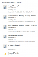
Obvious red flag #2 (note that none of these licenses and certs have even the slightest to do with semiconductors).
1678728936128.png
Dig into SemiAnalysis. It looks like a consulting start-up that Dylan himself started based on zero relevant professional experience.
 

HighGround

Senior Member
Registered Member
Dylan Patel is a new business school undergrad with no semiconductor experience. I don't trust anything he says that isn't corroborated by original literature and if it is then I could've just read the original literature.

Is there anything in there that can't be gained from open source AMAT literature?
I don't know, because I have no semiconductor experience either (or a degree for that matter). Which is why I rarely post in this thread, I spend most of my time reading a few hundred pages back.

Now not trusting him is fine, but to be fair I don't really find anything he says to be... particularly inaccurate or egregious. He tends to type out the right amount of disclaimers. For example, in this instance, he says the following in the first couple paragraphs.

Last week, Applied Materials, the 2nd largest semiconductor equipment manufacturer in the world, announced they have a potential solution. That solution is the Centura Sculpta tool, a new tool that can perform a new process step, “pattern shaping”. According to Applied Materials, the Sculpta tool could be used to reduce the use of EUV lithography by as much as HALF for some layers. If true, this would reshape the cost structure of the industry. There’s a lot of room to be skeptical of Applied Material’s claims, so let’s bring on the nuance for this discussion.

More importantly, Dylan Patel is very much a Western-style analyst. So his reports tend to be a good proxy for what the "West" thinks about a particular semiconductor issue. I thought you guys might find his insight on this new tool useful, even if it might be wrong.

A major reason of why I am on this forum, is so that I can expose myself to perspectives which greatly differ from what I usually read. I don't agree with a lot of takes on this Forum, but I am always happy to listen to the other side.
 

CMP

Senior Member
Registered Member
I don't know, because I have no semiconductor experience either (or a degree for that matter). Which is why I rarely post in this thread, I spend most of my time reading a few hundred pages back.

Now not trusting him is fine, but to be fair I don't really find anything he says to be... particularly inaccurate or egregious. He tends to type out the right amount of disclaimers. For example, in this instance, he says the following in the first couple paragraphs.


More importantly, Dylan Patel is very much a Western-style analyst. So his reports tend to be a good proxy for what the "West" thinks about a particular semiconductor issue. I thought you guys might find his insight on this new tool useful, even if it might be wrong.

A major reason of why I am on this forum, is so that I can expose myself to perspectives which greatly differ from what I usually read. I don't agree with a lot of takes on this Forum, but I am always happy to listen to the other side.
Nonsense. This isn't about sides. Dylan Patel doesn't have relevant education nor relevant professional experience prior to SemiAnalysis, where he instantly became Chief Analyst (likely a title he gave himself by virtue of it being his own consulting startup). I was a PM in hardware engineering (before switching to a much more profitable industry), and Dylan isn't even qualified to be an intern in semiconductor industry, let alone an analyst. Nobody will even hire him as a technician.
 

CMP

Senior Member
Registered Member
Did a deeper dive and I think it's a fair characterization to say that Dylan Patel is just an over glorified semiconductor industry journalist. Heavy emphasis on journalist. One that has a LOT of genuine passion, and does a LOT of reading and research, but is DEFINITELY not a former engineer at Nvidia, Intel, Qualcomm, LAM, Applied Materials, AMD, TSMC, Samsung, etc. working directly with either product or process. I worked with a former Nvidia engineering manager. I think it's fair to say that almost anyone with real insight knows better than to risk their careers talking openly about what they see in their work. They're all tied down with NDAs and would have any media interactions or publications pre-screened and approved internally by the relevant departments first.
 

latenlazy

Brigadier
Did a deeper dive and I think it's a fair characterization to say that Dylan Patel is just an over glorified semiconductor industry journalist. Heavy emphasis on journalist. One that has a LOT of genuine passion, and does a LOT of reading and research, but is DEFINITELY not a former engineer at Nvidia, Intel, Qualcomm, LAM, Applied Materials, AMD, TSMC, Samsung, etc. working directly with either product or process. I worked with a former Nvidia engineering manager. I think it's fair to say that almost anyone with real insight knows better than to risk their careers talking openly about what they see in their work. They're all tied down with NDAs and would have any media interactions or publications pre-screened and approved internally by the relevant departments first.
To be fair he still has a better technical grasp than most business side analysts or journalists who cover this stuff. But I agree once you get past a point there will be a limit to the amount of technical insight he can provide. Ultimately though for our purposes here the primary limitation in the value he can provide is simply that he does not follow the Chinese semis industry and doesn't seem to have much idea about where the baseline is with Chinese R&D.
 
Status
Not open for further replies.
Top