Chinese semiconductor industry

Status
Not open for further replies.

tonyget

Senior Member
Registered Member
it looks like he is saying that the existing 90nm ARF scanner can be used up to 65nm process. And that the new ICRD line is a 55nm process. Things that he say often contradict themselves, so I can only assume that ICRD is multi-patterning ARF dry scanner to do 55nm process.

I mean first he says that the ARF dry is for 55nm process at ICRD and it needs to be validated before mass production. Then he says ARF dry is for 90nm process and it is already mass produced with 10 U-Precision DWS supplied.

He just answered this question few minutes ago

你是魔鬼吗:啥情况,90nm光刻机是能做55nm的吗?
havok:可以。65nm和55nm用的是相同的设备,这2个节点上光刻真正能满足的是互连层,而对于小于互连层的更小尺度的线宽则需要配合光刻胶、材料、刻蚀等一些特殊的工艺手段巧妙实现

你是魔鬼吗:What's the situation, can the 90nm lithography machine do 55nm?
havok:Yes. 65nm and 55nm use the same equipment, the lithography on these two nodes can really satisfy the interconnection layer, and for the smaller-scale line width than the interconnection layer, it needs to cooperate with photoresist, material, etch and other special craft means to achieve ingeniously
 

Weaasel

Senior Member
Registered Member
I think people need to calm down again. I'm really annoyed to see this level of constant hyperventilation. Clearly, someone from SMEE cannot spell everything out for everyone. And frankly, I doubt any of us would understand it if he did. He does not seem to be concerned about mass production of this first generation DUVi machine. Which to me indicates that the project's success does not depend on U-precision piece for at least mass production of SSA800. So, please calm down everyone. The far more important step is having SMIC and others to do their validation of the production prototype and then to raise the production.
Which companies are presently among SMEE's most prominent customers of its currently sold lithography machined?
 

tonyget

Senior Member
Registered Member
你是魔鬼吗:那能做55nm逻辑工艺吗?
havok:逻辑工艺相对复杂一般需要NA0.85~0.93的干式光刻机做。

你是魔鬼吗:Can it do 55nm logic process?
havok:The logic process is relatively complicated and generally requires a dry lithography machine with NA0.85-0.93.
 

european_guy

Junior Member
Registered Member
He just answered this question few minutes ago

Please could you ask havoc if 90nm uses 0.75NA and immersion optic uses 0.85NA? Maybe 0.85NA is not enough for 28nm and also the 0.75NA maybe is too small if they do the 55nm with it.


EDIT: Ok, I see now your above reply. So it seems the dry version maybe is not 0.75NA as @hvpc reported....or otherwise the 55nm is not for logic.
 
Last edited:

hvpc

Junior Member
Registered Member
Please could you ask havoc if 90nm uses 0.75NA and immersion optic uses 0.85NA? Maybe 0.85NA is not enough for 28nm and also the 0.75NA maybe is too small if they do the 55nm with it.


EDIT: Ok, I see now your above reply. So it seems the dry version maybe is not 0.75NA as @hvpc reported....or otherwise the 55nm is not for logic.
I’m going off on what Havok said that the scanner has 90nm resolution capability.

0.75NA ArF scanner could do 90nm resolution;
0.85NA ArF scanner should be rated as 72nm resolution;
0.93NA ArF scanner is rated at 65nm resolution

since SMEE and Havok calls their dry ArF scanner the “90nm ArF dry” then that tool has to be 0.75NA.

second point, a tool with 90nm resolution will not be able to handle 65nm let along 55nm node’s most critical layer.

third point, SMEE published papers on SSA600 and indicated that it has 0.75NA projection lens, consistent with their claim of 90nm resolution. Now, if latest SMEE ArF has improved projection lens, then Havok is mistakenly still calling it “90nm ArF”. if the new ArF has 0.85 or 0.93 NA then these should have much better resolution limit than 90nm

so either Havok is confused with his facts or he is not aware of what actual fab needs.
 

tphuang

Lieutenant General
Staff member
Super Moderator
VIP Professional
Registered Member
I’m going off on what Havok said that the scanner has 90nm resolution capability.

0.75NA ArF scanner could do 90nm resolution;
0.85NA ArF scanner should be rated as 72nm resolution;
0.93NA ArF scanner is rated at 65nm resolution

since SMEE and Havok calls their dry ArF scanner the “90nm ArF dry” then that tool has to be 0.75NA.

second point, a tool with 90nm resolution will not be able to handle 65nm let along 55nm node’s most critical layer.

third point, SMEE published papers on SSA600 and indicated that it has 0.75NA projection lens, consistent with their claim of 90nm resolution. Now, if latest SMEE ArF has improved projection lens, then Havok is mistakenly still calling it “90nm ArF”. if the new ArF has 0.85 or 0.93 NA then these should have much better resolution limit than 90nm

so either Havok is confused with his facts or he is not aware of what actual fab needs.
I think he is trying to be contradicting with things he say in order to not release too much information and loose his job.

If I had to guess, there is a 90nm resolution in production already and another 65nm resolution version that's getting tested right now with ICRD which is still validating. Otherwise, some of his other comments don't make sense to me.
 

tokenanalyst

Brigadier
Registered Member

Huahai Qingken (Hwatsing) expects revenue in 2022 to be 1.53 billion to 1.695 billion yuan, a year-on-year increase of 90.09% to 110.59%​


According to news from Jiwei.com, on January 19, Huahai Qingke released the 2022 annual performance forecast, saying that according to preliminary calculations by the financial department, the company expects to achieve annual operating income of 1.53 billion to 1.695 billion yuan in 2022, an increase over the same period last year. 725.1195 million yuan to 890.1195 million yuan, a year-on-year increase of 90.09% to 110.59%.

In terms of net profit, Huahai Qingke expects to realize a net profit attributable to owners of the parent company of RMB 437.00 million to RMB 517.00 million in 2022, an increase of RMB 238.7233 million to RMB 318.7233 million compared with the same period of the previous year, and a year-on-year increase of 120.40% to 160.75%.

It is estimated that in 2022, the net profit attributable to the owners of the parent company after deducting non-recurring gains and losses will be 342.00 million to 400.00 million yuan, an increase of 228.024 million yuan to 286.024 million yuan compared with the same period of the previous year, and a year-on-year increase of 200.06% to 250.95 million yuan. %.

Huahai Qingke said that in 2022, the company actively grasped the market opportunities brought about by the demand pull of the integrated circuit industry, overcame the impact of unfavorable factors such as the epidemic situation and the supply chain, continued to increase R&D investment and production capacity construction, and strengthened the company's core competitiveness. CMP equipment and supporting services, wafer recycling business, etc. have achieved continuous growth throughout the year.

According to the data, Huahai Qingke Co., Ltd. is a high-end semiconductor equipment supplier with core independent intellectual property rights. Its main products include CMP equipment, thinning equipment, liquid supply system, wafer regeneration, key consumables and maintenance services.

Please, Log in or Register to view URLs content!
 

european_guy

Junior Member
Registered Member
I’m going off on what Havok said that the scanner has 90nm resolution capability.

0.75NA ArF scanner could do 90nm resolution;
0.85NA ArF scanner should be rated as 72nm resolution;
0.93NA ArF scanner is rated at 65nm resolution

since SMEE and Havok calls their dry ArF scanner the “90nm ArF dry” then that tool has to be 0.75NA.

second point, a tool with 90nm resolution will not be able to handle 65nm let along 55nm node’s most critical layer.

third point, SMEE published papers on SSA600 and indicated that it has 0.75NA projection lens, consistent with their claim of 90nm resolution. Now, if latest SMEE ArF has improved projection lens, then Havok is mistakenly still calling it “90nm ArF”. if the new ArF has 0.85 or 0.93 NA then these should have much better resolution limit than 90nm

so either Havok is confused with his facts or he is not aware of what actual fab needs.

Thanks for your reply. Yes it is not all so clear.

..but you added an interesting point.

If they really use the 65nm resolution with immersion to reach the 28nm node critical layers, it means that the immersion system should have 0.93NA. Correct?

So the 2 optic systems for Arf should be 0.75NA/0.85NA, what havoc calls 90nm resolution, and the 0.93NA that is supposed to correspond to the dry 65nm resolution system (38/45nm resolution with immersion).
 
Last edited:

tokenanalyst

Brigadier
Registered Member

Microelectronics has made progress in the field of binary neural network macro-level in-memory computing chip design​


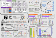
In recent years, non-volatile in-memory computing (nvCIM), as an emerging architecture, offers the possibility to handle data-intensive artificial intelligence (AI) tasks in edge systems with limited resources. In-memory computing technology based on resistive variable memory (RRAM) is a strong competitor to realize nvCIM. By deploying the weight matrix in the neural network to the RRAM cross array, using Ohm's law and Kirchhoff's law to accelerate the matrix-vector multiplication calculation, it can significantly reduce the data handling between the calculation and storage units, thereby increasing the system's inference speed and energy efficiency. However, the existing nvCIM architecture still has some challenges in matching edge AI systems: on the software side, due to the high precision required by traditional deep learning algorithms, resulting in increased storage and computing costs; on the hardware side, analog-to-digital converters (ADCs) and The use of peripheral circuits such as sense amplifiers (SA) greatly increases chip area and power consumption.

  In response to these problems, the team of Academician Liu Ming of the Key Laboratory of Microelectronic Devices and Integration Technology of the Institute of Microelectronics developed a digital RRAM macro-level memory computing chip (3T2R-Macro) for binary neural networks (BNN) (Figure 1a ). By using the voltage division principle to map the binary neural network weight matrix, the inverter is used to quantize the multiplication and addition calculation results into a stable voltage output. This design eliminates the peripheral ADC or SA, effectively reduces the chip area, energy consumption and delay, and improves the robustness to noise. The team also used the software-hardware collaborative design method to realize batch normalization (Batch Normalization) and activation function (Activation) calculation in the 3T2R-Macro on-chip binary convolutional neural network model by adjusting the power supply voltage of the inverter (Figure 1b ). The 3T2R-Macro design achieves recognition rates of 86.2% and 95.6% on the CIFAR-10 and MNIST datasets, respectively (Fig. 1c). The simulation results of the 180 nm process node show that the minimum calculation delay of the chip is 8 ns (Figure 1d), and the peak energy efficiency is 51.3 TOPS/W (Figure 1e). Compared with the reported current accumulation-based analog nvCIM design, 3T2R-Macro saves 10% of the chip area and 30% of the energy consumption of multiply-add calculations, and improves the system robustness by 20%. This research result provides an efficient solution for deploying AI tasks in edge systems with limited resources.

1674145083632.png

Please, Log in or Register to view URLs content!
 

FairAndUnbiased

Brigadier
Registered Member

Microelectronics has made progress in the field of binary neural network macro-level in-memory computing chip design​


In recent years, non-volatile in-memory computing (nvCIM), as an emerging architecture, offers the possibility to handle data-intensive artificial intelligence (AI) tasks in edge systems with limited resources. In-memory computing technology based on resistive variable memory (RRAM) is a strong competitor to realize nvCIM. By deploying the weight matrix in the neural network to the RRAM cross array, using Ohm's law and Kirchhoff's law to accelerate the matrix-vector multiplication calculation, it can significantly reduce the data handling between the calculation and storage units, thereby increasing the system's inference speed and energy efficiency. However, the existing nvCIM architecture still has some challenges in matching edge AI systems: on the software side, due to the high precision required by traditional deep learning algorithms, resulting in increased storage and computing costs; on the hardware side, analog-to-digital converters (ADCs) and The use of peripheral circuits such as sense amplifiers (SA) greatly increases chip area and power consumption.

  In response to these problems, the team of Academician Liu Ming of the Key Laboratory of Microelectronic Devices and Integration Technology of the Institute of Microelectronics developed a digital RRAM macro-level memory computing chip (3T2R-Macro) for binary neural networks (BNN) (Figure 1a ). By using the voltage division principle to map the binary neural network weight matrix, the inverter is used to quantize the multiplication and addition calculation results into a stable voltage output. This design eliminates the peripheral ADC or SA, effectively reduces the chip area, energy consumption and delay, and improves the robustness to noise. The team also used the software-hardware collaborative design method to realize batch normalization (Batch Normalization) and activation function (Activation) calculation in the 3T2R-Macro on-chip binary convolutional neural network model by adjusting the power supply voltage of the inverter (Figure 1b ). The 3T2R-Macro design achieves recognition rates of 86.2% and 95.6% on the CIFAR-10 and MNIST datasets, respectively (Fig. 1c). The simulation results of the 180 nm process node show that the minimum calculation delay of the chip is 8 ns (Figure 1d), and the peak energy efficiency is 51.3 TOPS/W (Figure 1e). Compared with the reported current accumulation-based analog nvCIM design, 3T2R-Macro saves 10% of the chip area and 30% of the energy consumption of multiply-add calculations, and improves the system robustness by 20%. This research result provides an efficient solution for deploying AI tasks in edge systems with limited resources.

View attachment 105473

Please, Log in or Register to view URLs content!
In memory computing is very promising because it can become another more than Moore gateway to high performance without having to participate in the die shrink rat race, and particularly, computing in 3D NAND lets you increase density by adding layers rather than die shrinking.

In my opinion it could be an entirely new paradigm. In addition you can have computing blocks, and memory blocks, integrated on the same die. Though you need an interconnect between them, it'll be an in chip connection rather than having to translate to i.e. PCIe.

Very interesting.
 
Status
Not open for further replies.
Top