Chinese semiconductor industry

Status
Not open for further replies.

Anlsvrthng

Captain
Registered Member
It’s not entirely a joke. State-of-the-art radars use 7nm and 5nm chips. Future applications of AI in weapon systems will require large computing and storage resources for training of deep learning models. AI at the edge often requires high power efficiency: nVidia recently demonstrated a 5nm inference chip for such applications.
Any link for 5/7 nm in radar applications?


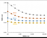
Problem with the low size nodes is the extreme cost of chip design.

And the extreme cost to make only few of them.
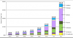
cost.png
run.png

A single 5 nm chip design cost as 5 F-35.

And if there is say 20 type of chips then the deisgn of all of them on 5nm will cost as much as 100 F-35.


If they want to re-design them because of mautring issues then they need to spend again that ammount of money. Instead to make, you know , fighter jets.

Reason why the military designs are 90 nm - 18 nm range. The cost to make smaller ICs prohibitivly high for small product run, it cheaper to make a bit bigger power supply in the missile than to spend extreme ammount of time and money for smaller nodes.
Risk is too high, consdiering that during the full system integration period they can find problems that require the full re-design of the ICs.
 

Gloire_bb

Captain
Registered Member
It’s not entirely a joke. State-of-the-art radars use 7nm and 5nm chips. Future applications of AI in weapon systems will require large computing and storage resources for training of deep learning models. AI at the edge often requires high power efficiency: nVidia recently demonstrated a 5nm inference chip for such applications.
Well, I heard the US have essentially forced an alternative high-end chip cluster to appear somewhere this forum is about.
 

olalavn

Senior Member
Registered Member
@olalavn @WTAN Sir, since SMEE SSA800 28nm DUVL theoretically can do 7nm using multi patterning (TSMC first gen 7nm was done using NXT 1980i) and Nata Optic had the Photoresist material needed to produce the chip, then we can assume an indigenous 7nm line is a possibility next year?

Please, Log in or Register to view URLs content!


Please, Log in or Register to view URLs content!

Please, Log in or Register to view URLs content!

Please, Log in or Register to view URLs content!

Please, Log in or Register to view URLs content!


Please, Log in or Register to view URLs content!

271 views1 hour ago
i just posted about 7nm photoresist rumors 2 days ago....
Screenshot 2022-11-28 183819.png
 
Last edited:

tphuang

Lieutenant General
Staff member
Super Moderator
VIP Professional
Registered Member
The military has been using commercial-off-the-shelf products for a long time now.

Xilinx’s 7nm Versal ACAP is used in radar applications:
Please, Log in or Register to view URLs content!


Intel’s Agilex on the Intel7 process has military applications like radar and EW systems listed as a use case.

A fully digital AESA with ultra low latency ADC converters in each T/R element and digital beam forming requires immense data throughout and processing capability. Because a huge amount of data processing is happening within the T/R elements in the array, energy efficiency is critical. This the reason why leading edge nodes are used in such applications.
This simply isn't true. You do not need 5/7 nm chips at all. CETC produces most of the chips for PLA. They are very high quality and I can assure you they are nowhere near 5/7 nm process. Do you think F-35 radar and mission computer use anything close to 5/7 nm chips?

GaN modules used in AESA radars are no where near leading node. I can assure you of that.
 

Maddy7881

New Member
Registered Member
i just posted about 7nm photoresist rumors 2 days ago....
View attachment 102597
It seems the lithography equipments will be the limiting factor in the mass production of 7 nm class processors. Besides , NAND and DRAM production also need to have access to latest NXT 2100i to have competitive products in the market. How many of the NXT 2100i have been delivered to China? And any prediction regarding the potential Q4 shipment. I fear, these will be restriction regarding the shipments of DUV scanners in coming months.
 

Zichan

Junior Member
Registered Member
This simply isn't true. You do not need 5/7 nm chips at all. CETC produces most of the chips for PLA. They are very high quality and I can assure you they are nowhere near 5/7 nm process. Do you think F-35 radar and mission computer use anything close to 5/7 nm chips?

GaN modules used in AESA radars are no where near leading node. I can assure you of that.
The sanctions are not so much about current weapon systems as they are about those in the near future. Think of fully digital AESA radars, counter LPI radar EW, AI at the edge. There is a huge difference in capability between something like the F-22 AESA radar with analog beamforming and the state-of-the-art fully digital radars. And I am not sure that we even have fully digital AESA radars at X-band yet. Which is why the US is determined to keep a tech gap with China by denying them access to leading edge manufacturing.

I’ve added a link to my answer with an example application of a 7nm ACAP device.
 
Last edited:

Anlsvrthng

Captain
Registered Member
The military has been using commercial-off-the-shelf products for a long time now.

Xilinx’s 7nm Versal ACAP is used in radar applications:
Please, Log in or Register to view URLs content!


Intel’s Agilex on the Intel7 process has military applications like radar and EW systems listed as a use case.

A fully digital AESA with ultra low latency ADC converters in each T/R element and digital beam forming (virtually unlimited number of beams on receive) requires immense data throughput and processing capability (space adaptive techniques to nullify jamming, etc). Because a huge amount of data processing is happening within the T/R elements in the array, energy efficiency is critical. This the reason why leading edge nodes are used in such applications.
That is an FPGA.

It is an off the shelf thingy, not a special military application IC.

Additionaly, it has way higher power consumption than the specific ICs.
 

Zichan

Junior Member
Registered Member
That is an FPGA.

It is an off the shelf thingy, not a special military application IC.

Additionaly, it has way higher power consumption than the specific ICs.
Read the article I linked. It illustrates a military application for that very SoC.
 
Status
Not open for further replies.
Top