Chinese semiconductor industry

Status
Not open for further replies.

NightFury1818

New Member
Registered Member
How much can AMAT, Lam, KLA be supplanted using equipment from TEL, Hitachi, Advantest etc (in conjunction with domestic firms)?

Also, how does SMIC make 7nm (N+2 process) or YMTC make 238 layers 3d nand without Synopsis and Cadence software? I thought Chinese EDA firms could cover only till 14nm
 

gelgoog

Lieutenant General
Registered Member
Software can be copied. Banning sales of US software to specific Chinese companies will only cause loss of sales revenue for US software vendors.
 

FairAndUnbiased

Brigadier
Registered Member
How much can AMAT, Lam, KLA be supplanted using equipment from TEL, Hitachi, Advantest etc (in conjunction with domestic firms)?

Also, how does SMIC make 7nm (N+2 process) or YMTC make 238 layers 3d nand without Synopsis and Cadence software? I thought Chinese EDA firms could cover only till 14nm
Everything else is OK but KLA. Advantest cannot replace KLA. Unfortunately KLA has a near monopoly on optical scatterometry for semiconductor QC and the only other company making it is Onto Innovation which is also US based. Everyone else (Chinese companies and Japanese companies like Hitachi) use CD-SEM which is much more expensive and requires vacuum handling i.e. loadlocks, pumps, vacuum grade materials, which imposes high cost and lowers throughput. You get much more detailed information from CD-SEM but that info is often unnecessary for QC alone.
 

theorlonator

Junior Member
Registered Member
Everything else is OK but KLA. Advantest cannot replace KLA. Unfortunately KLA has a near monopoly on optical scatterometry for semiconductor QC and the only other company making it is Onto Innovation which is also US based. Everyone else (Chinese companies and Japanese companies like Hitachi) use CD-SEM which is much more expensive and requires vacuum handling i.e. loadlocks, pumps, vacuum grade materials, which imposes high cost and lowers throughput. You get much more detailed information from CD-SEM but that info is often unnecessary for QC alone.
So no KLA means what for the near term?
 

olalavn

Senior Member
Registered Member
So no KLA means what for the near term?
28nm node optical measuring device was completed 2-3 months ago, I have posted on twitter, even 90nm lithography machine they also make 28nm chip... long term future they will be stable, i'm looking forward to next year they will reorganize their optical valleys, and instrumentation will be the main target
 

tokenanalyst

Brigadier
Registered Member
Everything else is OK but KLA. Advantest cannot replace KLA. Unfortunately KLA has a near monopoly on optical scatterometry for semiconductor QC and the only other company making it is Onto Innovation which is also US based. Everyone else (Chinese companies and Japanese companies like Hitachi) use CD-SEM which is much more expensive and requires vacuum handling i.e. loadlocks, pumps, vacuum grade materials, which imposes high cost and lowers throughput. You get much more detailed information from CD-SEM but that info is often unnecessary for QC alone.
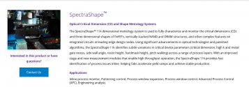
Well, Shanghai Jihnce and RSIC offer Optical metrology equipment probably using a technique similar to KLA for thin film measurement and CD measurement, IDK for overall QC control. So is good opportunity to break through that monopoly.

Please, Log in or Register to view URLs content!

Please, Log in or Register to view URLs content!

1666029816068.png
 

sndef888

Captain
Registered Member
So if I have this right, the latest round of sanctions is to cut off US equipment manufacturers, largely used in places like YMTC's NAND and CXMT's DRAM production, while ASML and Japanese equipment makers (excluding EUV) are still allowed to be sold as they don't exceed 25% US content, so SMIC can still continue expanding

Is this accurate?
 

FairAndUnbiased

Brigadier
Registered Member
Well, Shanghai Jihnce and RSIC offer Optical metrology equipment probably using a technique similar to KLA for thin film measurement and CD measurement, IDK for overall QC control. So is good opportunity to break through that monopoly.

Please, Log in or Register to view URLs content!

Please, Log in or Register to view URLs content!

View attachment 99620
Holy crap, this is amazing. I've always thought that nanoscale optical metrology was something out of reach for Chinese companies. To me optical CD is kind of like black magic because it isn't something you can directly understand, there's a ton of assumptions and theory behind it.
 

tokenanalyst

Brigadier
Registered Member
Holy crap, this is amazing. I've always thought that nanoscale optical metrology was something out of reach for Chinese companies. To me optical CD is kind of like black magic because it isn't something you can directly understand, there's a ton of assumptions and theory behind it.
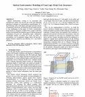
Its seem like some kind black magic, for measuring the thickness of a film is easier, in the lab is just checking the reflection in a color scale, but for measuring 3d structures is I guess is more complicated and more computational power is needed. Looks like KLA is using pretty advance technology to map the wafer but I still think is a pretty close technique to what Chinese companies are using.

1666033256636.png

Either way looks like the ICRD and Harbin are working in that area.

1666034609535.png


Please, Log in or Register to view URLs content!
 
Status
Not open for further replies.
Top