Very much this lol. The bottleneck is not availability of information but availability of *knowledge* to index the information.You need to understand the key parts of getting a CVD, ALD or even PVD instrument to work. Most people wouldn't think of a canister being important or how exactly precursors get delivered to a tool chamber.
When I was a TA in grad school a student complained that I solved his question by showing him a Google result. I said "if it was so easy then how come you didn't Google it yourself?" He said he didn't know what to search for. Exactly.
You are using an out of date browser. It may not display this or other websites correctly.
You should upgrade or use an alternative browser.
You should upgrade or use an alternative browser.
Chinese semiconductor industry
- Thread starter Hendrik_2000
- Start date
- Status
- Not open for further replies.
antiterror13
Brigadier
These links have some information about this product.
Some quotes:
"The manufacturer's next-generation KX-6000 CPU lineup will be replacing their KX-5000 and ZX-200 CPUs which have been on the market from 2017-2018. The latest chips are expected to feature 4 cores, 8 threads, up to 3.0 GHz clock speeds, DDR4 DRAM support, PCIe 3.0 I/O, and a homegrown 16nm architecture.
...
So coming back to the Zhaoxin KX-6000G CPUs which we may as well refer to as APUs since they utilize the same Zhaoxin-made ZX C1080 GPU that is featured on the Glenfly Arise-GT-10C0 dGPU
...
According to Zhaoxin, the CPU packs 8 cores and 16 threads which is made possible through fusing two dies on the same package. The standard version of the KX-6000 CPUs only comes with the C-960 integrated GPU that offers VGA, HDMI, DP support at up to 4K resolutions.
...
For starters, in 3DMark 11, the Zhaoxin integrated GPU scores around 1000 points which is an over 3x increase compared to the older GPU.
...
While it is a huge improvement over its predecessor, the integrated chip is still only on par with an NVIDIA GT 630 graphics card in the 3DMark 11 (Performance) benchmark which scores similar points.
...
As for the CPU, the Zhaxoin (sic) chip scores over 15,000 MIPS in multi-threading decompression which puts it faster than the AMD Ryzen 3 1300X and close to Intel's Core i5-7500."
The user comments are crap though.
Well, GT 630 graphics card and i5-7500 are sufficient for most employees and users .. a good start anyway
Optical wafer defect inspection at the 10 nm technology node and beyond
X-RAY CRITICAL DIMENSIONby International Journal of Extreme Manufacturing

Defect inspection scientists from Huazhong University of Science and Technology, Harbin Institute of Technology and The Chinese University of Hong Kong make a thorough review of new perspectives and exciting trends on the foundation of former great reviews in the field of defect inspection methods. The review focuses on three specific areas: (1) the defect detectability evaluation, (2) the diverse optical inspection systems, and (3) the post-processing algorithms.
Publishing in the journal International Journal of Extreme Manufacturing, the Nanoscale and Optical Metrology Research Center (NOMRC) led by Prof. Shiyuan Liu and Prof. Jinlong Zhu from Huazhong University of Science and Technology and their collaborators from Harbin Institute of Technology and The Chinese University of Hong Kong wrote the first systematic review to introduce the research background, discuss the latest progress and the trend of optical wafer defect inspection. This review has disclosed that cutting-edge techniques such as nanophotonics, optical vortices, computational imaging, quantitative phase imaging, and deep learning can make a profound impact on sub-10 nm defect inspection. The work may pave new avenues for the field of semiconductor wafer defect inspection.
Prof. Jinlong Zhu and Prof. Shiyuan Liu say that "the ever-shrinking features and space on patterned wafers would dramatically strain the capabilities of all the current metrology and inspection solutions in balancing sensitivity, specificity, process speed, and capture rate."
Optical far-field wafer inspection remains one of the workhorses for defect inspection in the fab. In a conventional defect inspection tool, the defects are captured by comparing circuit pattern images of adjacent dies. The first author of the review article, Prof. Jinlong Zhu says that "the key to defect inspection is not resolution, but the signal-to-noise ratio (SNR) and contrast. The improvement of SNR and contrast highly depends on sophisticated instruments, advanced modeling architectures and post-processing algorithms, all of which drove us to make a comprehensive review of wafer defect detection methods from the following three aspects: (1) the defect detectability evaluation, (2) the diverse optical inspection systems, and (3) the post-processing algorithms."
"It is of great importance to carry out defect detectability assessment for a specific type of inspection tools for advanced nodes," co-first author Dr. Jiamin Liu explained. "In fact, the evaluation of defect detectability usually involves the formulation of quantitative rules for the SNR of the defect scattering signals, the development of simulation tools for defect scattering signals modeling, and the analysis of defect SNR. We found the defect SNR depends significantly on material and defect topology."+
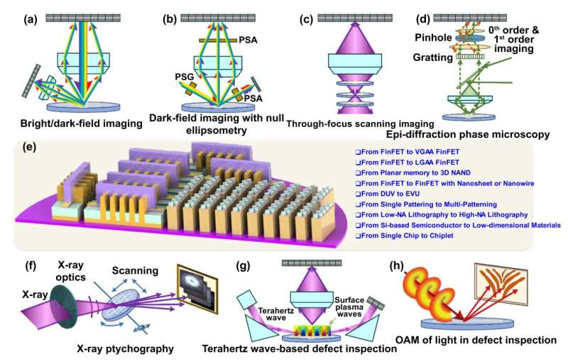
The conventional approaches in optical defect inspection, such as the amplitude-based one alongside its post-processing algorithms, has been thoroughly discussed. The novel inspection mechanisms including phase-, orbital angular momentum-, terahertz wave-, and hyperbolic Bloch modes-based ones, have been highlighted to remind readers of their potentials in opening up new directions in the field. Besides, X-ray ptychography, the only optical method that can directly image both surface and undersurface sub-20 nm defects for the entire wafer, has also been reviewed and prospected in detail in the article. X-ray ptychography has the potential to penetrate the field by providing revolutionary 3D resolution and sensitivity once the drawbacks including the synchrotron X-ray light source, a massive amount of data, and the low speed being conquered in the future.
"Whether it is the simplest image difference operator or the complex image synthetic algorithm or even the deep learning algorithms, these post-processing algorithms play a critical role in optical defect inspection in terms of improving SNR and contrast of defects. Therefore, we provided a detail discussion of post-processing algorithms involved in patterned wafer defect inspection with a specific focus on the advantages and disadvantages of deep learning algorithms," co-first author Dr. Tianlai Xu further added.
Well, GT 630 graphics card and i5-7500 are sufficient for most employees and users .. a good start anyway
Now is the matter if zhaoxin being able to get it produce at a semi competitive price. Low wattage would also be beneficial.
I think the GPU in the benchmark is not a card but is integrated with the CPU in the same SOC (an APU). That will put it similar to Intel integrated solutions I guess.Well, GT 630 graphics card and i5-7500 are sufficient for most employees and users .. a good start anyway
Probably they are related to this Chinese company who do X-Ray metrology.Optical wafer defect inspection at the 10 nm technology node and beyond
X-RAY CRITICAL DIMENSION
by International Journal of Extreme Manufacturing
Diverse optical wafer defect inspection systems including (a) Brightfield/darkfield imaging system, (b) Dark-field imaging with null ellipsometry, (c) Through-focus scanning imaging microscopy, (d) Epi-diffraction phase microscopy, (e) Patterned wafer containing logic dies and 3D NAND memory dies, (f) X-ray ptychography, (g) THz wave-based defect inspection system, and (h) Coherent Fourier scatterometry techniques using different OAM illumination beams. Credit: By Jinlong Zhu et al
Defect inspection scientists from Huazhong University of Science and Technology, Harbin Institute of Technology and The Chinese University of Hong Kong make a thorough review of new perspectives and exciting trends on the foundation of former great reviews in the field of defect inspection methods. The review focuses on three specific areas: (1) the defect detectability evaluation, (2) the diverse optical inspection systems, and (3) the post-processing algorithms.
Publishing in the journal International Journal of Extreme Manufacturing, the Nanoscale and Optical Metrology Research Center (NOMRC) led by Prof. Shiyuan Liu and Prof. Jinlong Zhu from Huazhong University of Science and Technology and their collaborators from Harbin Institute of Technology and The Chinese University of Hong Kong wrote the first systematic review to introduce the research background, discuss the latest progress and the trend of optical wafer defect inspection. This review has disclosed that cutting-edge techniques such as nanophotonics, optical vortices, computational imaging, quantitative phase imaging, and deep learning can make a profound impact on sub-10 nm defect inspection. The work may pave new avenues for the field of semiconductor wafer defect inspection.
Prof. Jinlong Zhu and Prof. Shiyuan Liu say that "the ever-shrinking features and space on patterned wafers would dramatically strain the capabilities of all the current metrology and inspection solutions in balancing sensitivity, specificity, process speed, and capture rate."
Optical far-field wafer inspection remains one of the workhorses for defect inspection in the fab. In a conventional defect inspection tool, the defects are captured by comparing circuit pattern images of adjacent dies. The first author of the review article, Prof. Jinlong Zhu says that "the key to defect inspection is not resolution, but the signal-to-noise ratio (SNR) and contrast. The improvement of SNR and contrast highly depends on sophisticated instruments, advanced modeling architectures and post-processing algorithms, all of which drove us to make a comprehensive review of wafer defect detection methods from the following three aspects: (1) the defect detectability evaluation, (2) the diverse optical inspection systems, and (3) the post-processing algorithms."
"It is of great importance to carry out defect detectability assessment for a specific type of inspection tools for advanced nodes," co-first author Dr. Jiamin Liu explained. "In fact, the evaluation of defect detectability usually involves the formulation of quantitative rules for the SNR of the defect scattering signals, the development of simulation tools for defect scattering signals modeling, and the analysis of defect SNR. We found the defect SNR depends significantly on material and defect topology."+
The conventional approaches in optical defect inspection, such as the amplitude-based one alongside its post-processing algorithms, has been thoroughly discussed. The novel inspection mechanisms including phase-, orbital angular momentum-, terahertz wave-, and hyperbolic Bloch modes-based ones, have been highlighted to remind readers of their potentials in opening up new directions in the field. Besides, X-ray ptychography, the only optical method that can directly image both surface and undersurface sub-20 nm defects for the entire wafer, has also been reviewed and prospected in detail in the article. X-ray ptychography has the potential to penetrate the field by providing revolutionary 3D resolution and sensitivity once the drawbacks including the synchrotron X-ray light source, a massive amount of data, and the low speed being conquered in the future.
"Whether it is the simplest image difference operator or the complex image synthetic algorithm or even the deep learning algorithms, these post-processing algorithms play a critical role in optical defect inspection in terms of improving SNR and contrast of defects. Therefore, we provided a detail discussion of post-processing algorithms involved in patterned wafer defect inspection with a specific focus on the advantages and disadvantages of deep learning algorithms," co-first author Dr. Tianlai Xu further added.

A Chinese quote to start your day especially me after partying all night and having a hangover!
"A leader is best when people barely know he exists, when his work is done, his aim fulfilled, they will say: we did it ourselves." by LAO TZU
18 hours ago — Asia tech 'godfathers' to decide US chips fate. US 'friendshoring' and Chips 4 alliance may or may not lure region's semiconductor heavies ...
Zhaoxin does okay in CPU front. There is that 50 million domestic order that will be filled over time. It's #2 in the domestic market after Phytium. At this point, Loongson is basically getting no orders domestically. I'd bet Phytium over Zhaoxin at this point, since D3000 should come out soon. Although in long term, maybe the domestic RISC-V chip makers will fare the best.These links have some information about this product.
Some quotes:
"The manufacturer's next-generation KX-6000 CPU lineup will be replacing their KX-5000 and ZX-200 CPUs which have been on the market from 2017-2018. The latest chips are expected to feature 4 cores, 8 threads, up to 3.0 GHz clock speeds, DDR4 DRAM support, PCIe 3.0 I/O, and a homegrown 16nm architecture.
...
So coming back to the Zhaoxin KX-6000G CPUs which we may as well refer to as APUs since they utilize the same Zhaoxin-made ZX C1080 GPU that is featured on the Glenfly Arise-GT-10C0 dGPU
...
According to Zhaoxin, the CPU packs 8 cores and 16 threads which is made possible through fusing two dies on the same package. The standard version of the KX-6000 CPUs only comes with the C-960 integrated GPU that offers VGA, HDMI, DP support at up to 4K resolutions.
...
For starters, in 3DMark 11, the Zhaoxin integrated GPU scores around 1000 points which is an over 3x increase compared to the older GPU.
...
While it is a huge improvement over its predecessor, the integrated chip is still only on par with an NVIDIA GT 630 graphics card in the 3DMark 11 (Performance) benchmark which scores similar points.
...
As for the CPU, the Zhaxoin (sic) chip scores over 15,000 MIPS in multi-threading decompression which puts it faster than the AMD Ryzen 3 1300X and close to Intel's Core i5-7500."
The user comments are crap though.
Aside from that, it's kind of nonsensical to see Zhaoxin attempt GPU. I really must ask why they are doing this. There are so many domestic GPU firms working on great design right now. Maybe they are focused on AI chips, but they will get to GPUs for personal computers soon enough. This Zhaoxin effort is just not competitive.
This sounds promising
Tech war: China chip start-ups clamour to tout AI chip breakthroughs after Nvidia sales ban, prompting analyst scepticism
Chinese semiconductor start-ups are rushing to claim breakthroughs in artificial intelligence (AI) chips after the US restricted the export of advanced chips from Nvidia Corp and Advanced Micro Devices (AMD) to China, prompting scepticism from many industry analysts.
- Chongqing-based Xiangdixian Computing Technology has unveiled Tianjun No. 1, a GPU with 12-nanometre node technology
Chongqing-based Xiangdixian Computing Technology, which designs microprocessors, this week unveiled Tianjun No. 1, a graphics processing unit (GPU) with 12-nanometre node technology. The company claimed it has “reached an internationally advanced level” and will “effectively fill the gap in the domestic market”, according to an official post on its WeChat account on Wednesday.
Xiangdixian, a chip design start-up founded in Chongqing, southwestern Sichuan Province in 2020, is headed by chip veteran Tang Zhimin who previously worked for Loongson Technology and Hygon Information Tech, two Chinese chip companies that make microprocessors.
12 nm, so this can easily be produced by the mature 14/12 nm process that SMIC has.
It seems like they have quite a few partners. I don't see how this is an AI GPU. This seems to be a produce for desktop market.
Says that Tianjun-1 is being tested out with CPUs from Loongson, Zhaoxin, Hygon, Sunway and Kunpeng. Interesting that Phytium is missing there. not sure who they are working with.天钧一号GPU也正在与龙芯、兆芯、海光、申威、鲲鹏等国产CPU进行适配工作
There does seem to be a couple of design house working on desktop GPUs now, so will be interesting who wins out.
The more famous one is Moore Threads and MTT S60.
that one is also using 12 nm technology, but can do 6 TFLOPS of calculates, which is more than the 4 TFLOPS for Tianjun-1.
I feel like long term, the ones that will win out will be the ones that capture the domestic AI GPU market and have the resources to move into the desktop GPU space.
We are definitely headed to a huge market downturn overall and in semiconductor industry.
Micron is planning 50% spending cut.
lol, Nvidia GPU demand crashed due to the crypto crash
You may want to say that SMIC is having problems, but they are not cutting back on planned fabs. Same with a lot of these other chinese chip makers. I'm not sure you can say the same about chipmakers and IDMs outside of China.
Looks like Nvidia greed finally catch up with them, they didn't give rat piss when their main costumers, gamers, were crying for affordable GPUs, now they want the same gamers to buy expensive cards that were destined to miners before the crash in first place.lol, Nvidia GPU demand crashed due to the crypto crash
But you know what? Nvidia fanboys still going to buy it.
- Status
- Not open for further replies.
