You are using an out of date browser. It may not display this or other websites correctly.
You should upgrade or use an alternative browser.
You should upgrade or use an alternative browser.
Chinese semiconductor industry
- Thread starter Hendrik_2000
- Start date
- Status
- Not open for further replies.
but it takes time for the optics and the rest to mature... even though China has a prototype... but the light source is weak and unstable..
China already has a patent on a 30kW CO2 MOPA laser. They wouldn't file a patent application unless they already had a working prototype. The fact the IOE had a working debris vacuum as part of the 2017 EUV prototype 5 years ago means this 30kW laser is probably already well into R&D with droplet sizes and illumination intervals. I wouldn't be surprised if they already have conversion efficiencies approaching 4%.The project "Research on vacuum system and mechanics of EUV lithography principle experimental device" carried out by Institute of Optoelectronics Technology, Chinese Academy of Sciences has successfully completed in-situ testing before acceptance test at Changchun Institute of Optics and Mechanics, the master unit of the project.View attachment 98159
I can understand if the light source were considered unstable, but being called weak is definitely very interesting considering 30kW is nearing the frontier for this kind of amplified laser. I think maybe the information you're mentioning might be referring to the entire integrated light source and perhaps comparing conversion efficiencies between Cymer, Gigaphoton and IOE (CAS) light sources? I know most of the problems relate to the debris cloud and premature pellicle contamination directly related to this. Is this what they mean when they say the light source is weak?
Okay I know it's not an official confirmation and coming from YT its more a speculation BUT the video do have a point.
1) Huawei IDM dream had been realized thanks to Uncle Sam, being the vanguard and helping develop domestic substitution and investing in critical tech like laser and EDA.
2) SMIC and HUAWEI had a good and friendly relationship and had collaborate, helping each other clandestinely.
3) helping SMIC build a wafer plant and negotiating TSMC supply chain partners.
4) Hisilicon will be releasing 2 processors these year 1) Kirin 830 and 2) Kirin 720 both using14nm domestic process. (use For the Return of The King baby!!!! )
)
5) Huawei had set up Precision Instrument Manufacturing Enterprise in 2021. Confirming @olalavn previous post about Huawei involving itself in developing a DUVL (maybe the rumored 22nm DUVL) and other core tech equipment.
1) Huawei IDM dream had been realized thanks to Uncle Sam, being the vanguard and helping develop domestic substitution and investing in critical tech like laser and EDA.
2) SMIC and HUAWEI had a good and friendly relationship and had collaborate, helping each other clandestinely.
3) helping SMIC build a wafer plant and negotiating TSMC supply chain partners.
4) Hisilicon will be releasing 2 processors these year 1) Kirin 830 and 2) Kirin 720 both using14nm domestic process. (use For the Return of The King baby!!!!
5) Huawei had set up Precision Instrument Manufacturing Enterprise in 2021. Confirming @olalavn previous post about Huawei involving itself in developing a DUVL (maybe the rumored 22nm DUVL) and other core tech equipment.
19 views6 minutes ago
I thought AMEC is the sole Chinese Etching equipment maker BUT I was wrong there is another one CHINA MICRO CORP and they also have in their product line up a 5nm capable Etching machine, with this coupled with ASML NXT 2050i and in the future NXT 2100i then a N+3 5nm chip is on the horizon.  Love the way the author of this article describe it, he wrote it with a lot of patriotic fervor....lol Jia You!!!!
It is conceivable that when the chip process of manufacturers such as SMIC develops to the 5nm process, at least there is no need to worry about facing the problem of "cutting supply" in terms of etching equipment.

According to the latest market news, on April 6, my country's well-known semiconductor equipment manufacturer China Micro Corporation (hereinafter referred to as "China Micro") publicly announced that the plasma etching equipment produced by the company has been applied to international first-line customers from 65 nanometers. To 5 nanometers and other advanced integrated circuit manufacturing production lines and advanced packaging production lines.
Wherein the micro its high-profile 12 inches high etching apparatus , it has been incorporated . 5 nm and less chip core components of the processing step .
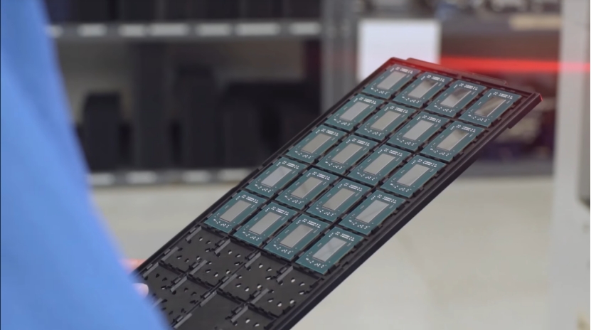
As we all know, there are only two foundries that can produce 5nm chips in the world, TSMC and Samsung. China Micro's statement is undoubtedly showing that the company's 12-inch high-end etching equipment has obtained the "seal certification" of the most advanced chip manufacturer in the world. In April last year, China Micro Corporation revealed that the company's high-end etching equipment won bulk orders from international customers.
The chip production of a company involves the supply of hundreds of equipment and parts. For example, since the United States is still unwilling to relax restrictions on EUV lithography machines, SMIC's 7nm and below process chip production cannot be carried out either. At the moment, the major breakthroughs made by high-end etching equipment in China and Microelectronics have undoubtedly ushered in a glimmer of light for the problem of "stuck necks" in my country's chips.
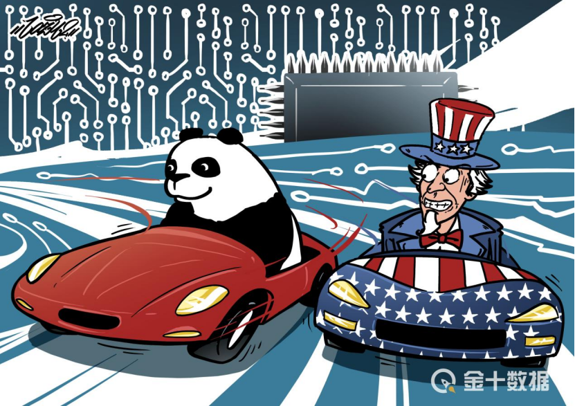
It is understood that in the entire process of chip manufacturing, etching equipment, photolithography equipment, and thin film deposition equipment are the most important three types of equipment. Among them, the etching equipment is more valuable than the lithography equipment we are familiar with. It is the most "burning" expense of a chip factory. The value of wafer manufacturing equipment accounts for 24% , and the lithography equipment is 23%.
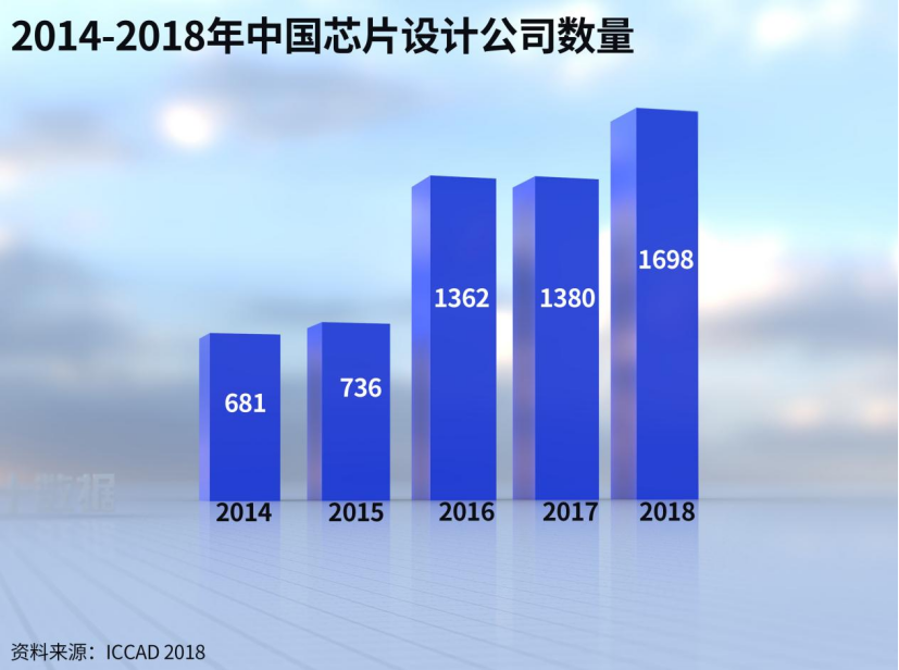
China Micro's financial report data shows that the company's etching equipment earned nearly 1.29 billion yuan in revenue in 2020, a year-on-year increase of about 58.49%.
It is conceivable that when the chip process of manufacturers such as SMIC develops to the 5nm process, at least there is no need to worry about facing the problem of "cutting supply" in terms of etching equipment.
It is conceivable that when the chip process of manufacturers such as SMIC develops to the 5nm process, at least there is no need to worry about facing the problem of "cutting supply" in terms of etching equipment.
Can produce 5nm chips!High-end etching equipment of Chinese companies unveiled and was "stamped" by Samsung and TSMC

According to the latest market news, on April 6, my country's well-known semiconductor equipment manufacturer China Micro Corporation (hereinafter referred to as "China Micro") publicly announced that the plasma etching equipment produced by the company has been applied to international first-line customers from 65 nanometers. To 5 nanometers and other advanced integrated circuit manufacturing production lines and advanced packaging production lines.
Wherein the micro its high-profile 12 inches high etching apparatus , it has been incorporated . 5 nm and less chip core components of the processing step .

As we all know, there are only two foundries that can produce 5nm chips in the world, TSMC and Samsung. China Micro's statement is undoubtedly showing that the company's 12-inch high-end etching equipment has obtained the "seal certification" of the most advanced chip manufacturer in the world. In April last year, China Micro Corporation revealed that the company's high-end etching equipment won bulk orders from international customers.
The chip production of a company involves the supply of hundreds of equipment and parts. For example, since the United States is still unwilling to relax restrictions on EUV lithography machines, SMIC's 7nm and below process chip production cannot be carried out either. At the moment, the major breakthroughs made by high-end etching equipment in China and Microelectronics have undoubtedly ushered in a glimmer of light for the problem of "stuck necks" in my country's chips.

It is understood that in the entire process of chip manufacturing, etching equipment, photolithography equipment, and thin film deposition equipment are the most important three types of equipment. Among them, the etching equipment is more valuable than the lithography equipment we are familiar with. It is the most "burning" expense of a chip factory. The value of wafer manufacturing equipment accounts for 24% , and the lithography equipment is 23%.

China Micro's financial report data shows that the company's etching equipment earned nearly 1.29 billion yuan in revenue in 2020, a year-on-year increase of about 58.49%.
It is conceivable that when the chip process of manufacturers such as SMIC develops to the 5nm process, at least there is no need to worry about facing the problem of "cutting supply" in terms of etching equipment.
Last edited:
Question can a DUVL produce a 3nm chip? I ask because after reading the spec of NXT 2100i provided by my mentor @hvpc maybe it can?
NXT:2100i makes a 20% step in on product overlay vs the NXT:2050i for a typical DRAM application 29 Sept. 2021 Slide 14 Improved scanner metrology software Improved setup repro for overlay Wafer table Improved overlay & lifetime improvements Projection optics Improved lens and cross matching control Optical sensors improved camera & thermal conditioning Alignment 12 colors 65 marks, small marks, combined layout Reticle handler Faster conditioning and lower reticleto-reticle temperature variation 2D Reticle stage grid calibration Reducing impact of reticle load errors on overlay NXT:2100i Throughput ≥295wph MMO ≤1.3nm On Product Overlay ≤1.4nm (DRAM) Overlay Productivity Public NXT platform reduces capital investment, fab
NXT:2100i makes a 20% step in on product overlay vs the NXT:2050i for a typical DRAM application 29 Sept. 2021 Slide 14 Improved scanner metrology software Improved setup repro for overlay Wafer table Improved overlay & lifetime improvements Projection optics Improved lens and cross matching control Optical sensors improved camera & thermal conditioning Alignment 12 colors 65 marks, small marks, combined layout Reticle handler Faster conditioning and lower reticleto-reticle temperature variation 2D Reticle stage grid calibration Reducing impact of reticle load errors on overlay NXT:2100i Throughput ≥295wph MMO ≤1.3nm On Product Overlay ≤1.4nm (DRAM) Overlay Productivity Public NXT platform reduces capital investment, fab
Question can a DUVL produce a 3nm chip? I ask because after reading the spec of NXT 2100i provided by my mentor @hvpc maybe it can?
NXT:2100i makes a 20% step in on product overlay vs the NXT:2050i for a typical DRAM application 29 Sept. 2021 Slide 14 Improved scanner metrology software Improved setup repro for overlay Wafer table Improved overlay & lifetime improvements Projection optics Improved lens and cross matching control Optical sensors improved camera & thermal conditioning Alignment 12 colors 65 marks, small marks, combined layout Reticle handler Faster conditioning and lower reticleto-reticle temperature variation 2D Reticle stage grid calibration Reducing impact of reticle load errors on overlay NXT:2100i Throughput ≥295wph MMO ≤1.3nm On Product Overlay ≤1.4nm (DRAM) Overlay Productivity Public NXT platform reduces capital investment, fab
Not according to the roadmap. But according to the roadmap, the most advanced chip they can produce is equivalent to the Samsung 4 nm and TSMC N5P. That should be advanced enough until 2026.
At this point, I'm more concerned about SMIC getting enough machines to expand their advanced node production than whether or not they are capable of producing advanced node. So, the Chinese equipment suppliers like AMEC need to really increase their production even more.
Last edited:
Do you mean that you are more concerned about SMIC getting enough machines to expand their CURRENT available (in their own possession) advanced node production AS COMPARED to more advanced nodes that are NOT presently in their possession?At this point, I'm more concerned about SMIC getting enough machines to expand their advanced node production than whether or not they are capable of producing advanced node. So, the Chinese equipment suppliers like AMEC need to really increase their production even more
China Micro is the same company as AMEC, aka. AMEC/Zhongwei/China Micro. Besides AMEC, the other companies I know of working on etch equipment are Naura/Huachuang and ACM/Shengmei. Naura/Huachuang has etch equipment for 14nm in the field and developing for 7nm. ACM/Shengmei is strictly wet etch so they are basically a non-factor.I thought AMEC is the sole Chinese Etching equipment maker BUT I was wrong there is another one CHINA MICRO CORP and they also have in their product line up a 5nm capable Etching machine, with this coupled with ASML NXT 2050i and in the future NXT 2100i then a N+3 5nm chip is on the horizon.Love the way the author of this article describe it, he wrote it with a lot of patriotic fervor....lol Jia You!!!!
Question can a DUVL produce a 3nm chip? I ask because after reading the spec of NXT 2100i provided by my mentor @hvpc maybe it can?
NXT:2100i makes a 20% step in on product overlay vs the NXT:2050i for a typical DRAM application 29 Sept. 2021 Slide 14 Improved scanner metrology software Improved setup repro for overlay Wafer table Improved overlay & lifetime improvements Projection optics Improved lens and cross matching control Optical sensors improved camera & thermal conditioning Alignment 12 colors 65 marks, small marks, combined layout Reticle handler Faster conditioning and lower reticleto-reticle temperature variation 2D Reticle stage grid calibration Reducing impact of reticle load errors on overlay NXT:2100i Throughput ≥295wph MMO ≤1.3nm On Product Overlay ≤1.4nm (DRAM) Overlay Productivity Public NXT platform reduces capital investment, fab
I guess this is the presentation you refer to:
It was part of last year's investor days at ASML:
This year it will be November 11
In my non-expert opinion, I think DUV 3nm is dead on arrival. However, it is doable IF you ignore yield issues, power consumption and the only goals are equivalent density and performance metrics. The amount of equipment you need after 28nm, aside from wafer specific equipment, almost doubles for every node for certain key equipment. So, 3nm node would need over 10 times as much equipment as a 28nm fab per wafer. You would need literally something like 1000+ etchers for a typical fab, it's just nuts. The economics make no sense, especially given that EUV already has superior price-performance at 7nm.Question can a DUVL produce a 3nm chip? I ask because after reading the spec of NXT 2100i provided by my mentor @hvpc maybe it can?
NXT:2100i makes a 20% step in on product overlay vs the NXT:2050i for a typical DRAM application 29 Sept. 2021 Slide 14 Improved scanner metrology software Improved setup repro for overlay Wafer table Improved overlay & lifetime improvements Projection optics Improved lens and cross matching control Optical sensors improved camera & thermal conditioning Alignment 12 colors 65 marks, small marks, combined layout Reticle handler Faster conditioning and lower reticleto-reticle temperature variation 2D Reticle stage grid calibration Reducing impact of reticle load errors on overlay NXT:2100i Throughput ≥295wph MMO ≤1.3nm On Product Overlay ≤1.4nm (DRAM) Overlay Productivity Public NXT platform reduces capital investment, fab
DUV multi-patterning is typically variations of LELE and SADP patterning. At 14nm you have proponents of either LELE or SADP. Once you move beyond 14nm, all processes are basically stacked SADP. So, 7nm would be SADP+SADP such that 3nm would be something like SADP+SADP+SADP+SADP+SADP.
When it comes to DUV, packaging is unquestionably the way to go. Absent EUV, China is going to get stuck at the equivalent of 5nm EUV when it comes to DUV scaling. I'm sure China will have a plethora of commercially available 7nm DUV designs. It's questionable though whether China will ever release commercially viable 7nm 2.5D/3D chips even though I am sure they will be developed. Once DUV 7nm 2.5D/3D chips are developed, we're talking about something around ~2026 which is around when China's EUV will be arriving. In other words, I think China will basically stop scaling DUV designs at 7nm and 14nm 2.5D/3D before China's EUV takes over.
- Status
- Not open for further replies.
