Chinese semiconductor industry

Status
Not open for further replies.

tokenanalyst

Brigadier
Registered Member

Zhongguo Optoelectronics has delivered nano-scale patterned wafer defect inspection equipment to customers​


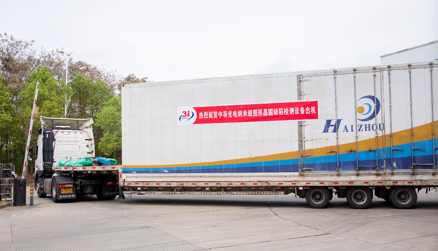
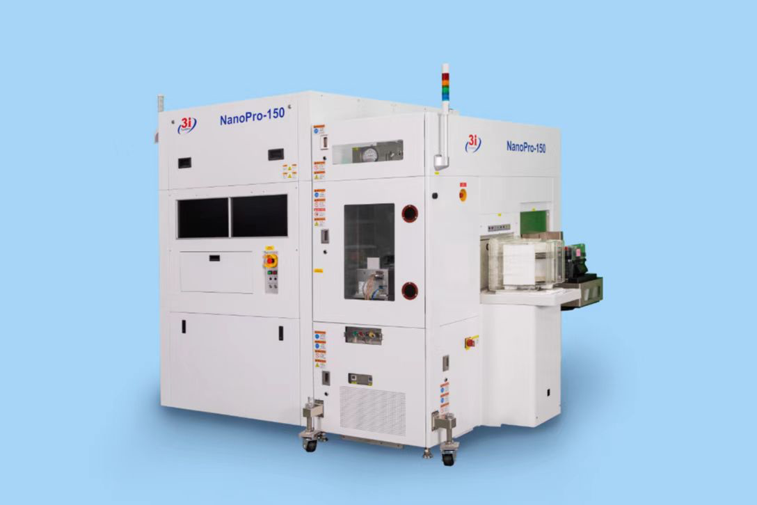
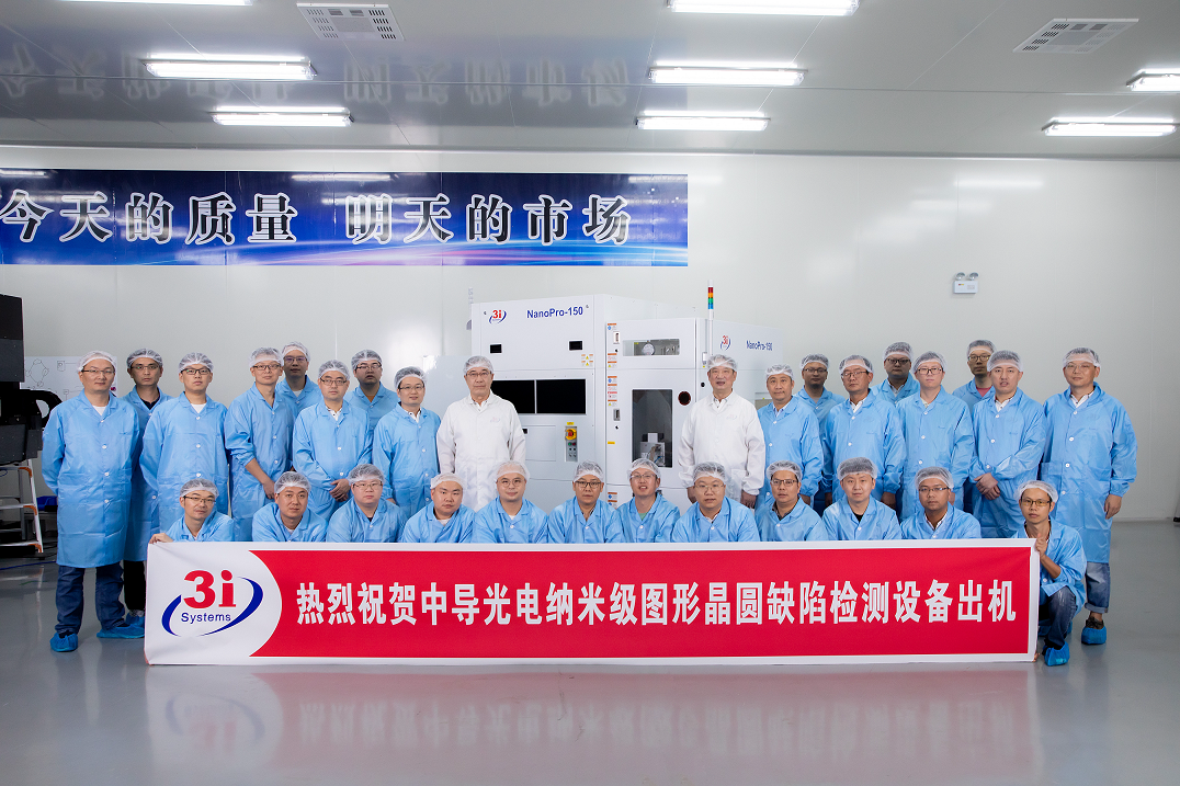
A few days ago, NanoPro-150, a "nano-scale patterned wafer defect inspection equipment" developed and manufactured by China Conductive Optoelectronics Equipment Co., Ltd. ("China Conductive Optoelectronics"), was delivered to the customer's factory. The customer is joined and guided by a domestic semiconductor chip manufacturing giant, and is a well-known enterprise in the domestic IGBT manufacturing field.
999953288908.3601855200811976.1652.png


It is reported that the NanoPro-1XX product series of Zhongguo Optoelectronics has a maximum sensitivity of 100nm, which is suitable for the manufacturing process requirements of semiconductor chips of 0.13μm-0.18μm and above. In addition to being similar to similar products from international top companies in terms of sensitivity, detection speed (Throughput) and other main performance parameters, this product series also has a number of unique innovations and features: First, it integrates "Bright Field" and "Dark Field". /Dark Field” in one, which not only ensures the inspection requirements for key processes such as lithography and etching, but also provides cost-effective inspection solutions for processes such as coating, CMP, and bare chips, which greatly expands the application scenarios of the equipment. The cost of use (COO) of the equipment is reduced; second, the "multi-channel imaging (MCI) technology" is adopted to improve the detection sensitivity of the equipment to different "detected materials/objects", and solve the "film color change/Color Variation" "interference to detection; third, the use of "dynamic image resolution extension (HDR)" technology to better solve the "light and dark contrast" problem of "metal-non-metal" mixed surfaces; fourth, according to customer needs, the device Compatible with two different wafer sizes, such as 8-inch and 12-inch, 6-inch and 8-inch, 5-inch and 6-inch, etc., which expands the scope of equipment use; fifth, integrates a large number of advanced image recognition and artificial intelligence software technology, and can match with the general software system and information exchange system of the international semiconductor manufacturing industry.
514792249859.4466.png


Compared with "unpatterned wafer defect inspection equipment", the technical difficulty of "patterned wafer defect inspection equipment" has been greatly improved, the scope of application is wider, and the economic value and market space of the product are also the same as "patterned wafer defect inspection equipment". several times. It is understood that the NanoPro-150 model delivered this time is a breakthrough in the localization of pattern inspection equipment in the domestic semiconductor front-end process.

Zhongguo Optoelectronics is a professional company specializing in the research, development and industrialization of high-end defect detection equipment in the front-end of the semiconductor industry. In the 16 years since its establishment, Zhongguo Optoelectronics has sold nearly 300 sets of various sub-micron (>0.5μm) "patterned" inspection equipment in the flat panel display (FPD) and other industrial fields. The company has undertaken dozens of national "863 plan" scientific research projects, scientific research projects of the Ministry of Industry and Information Technology, provincial and municipal scientific research projects, and has accumulated rich experience in the research and development and industrialization of high-end semiconductor testing equipment. Alternative suppliers.

The NanoPro-2XX series products of Zhongguo Optoelectronics have a maximum sensitivity of about 70nm and are suitable for 60nm-90nm semiconductor processes; its NanoPro-3XX series products have a maximum sensitivity of about 40nm and are suitable for 45nm-60nm semiconductor processes. NanoPro-2XX series products will accept customer orders next year, and NanoPro-3XX will also complete the research and development later and accept customer evaluation. The NanoPro-1XX series products and MDI sub-micron testing equipment that CND is currently in sales and mass production, plus NanoPro-2XX and NanoPro-3XX will enter the market successively, which can cover more than 90% of the domestic semiconductor front-end testing equipment demand market , bringing dawn to the localization of testing equipment in China's semiconductor industry.
1138294236473.1987.png


Please, Log in or Register to view URLs content!
 

horse

Colonel
Registered Member
It baffles me, China is reluctant to Tit for Tat policy. NVidia and AMD makes most of their money from China. If they don’t sell high end chips, then simply ban their low end chips too. China is basically funding Western chips development by procuring low end chips while their own domestic chips industries suffer. When money dries up, western companies need to shed workforce/high end research to keep cost down and make shareholders happy.

Technological diversion is also another potential gamble if you want to catch up to the front runner. Just hope western tech ecosystem plateau and your alternative path is the most sensible path forward. Just like Huwaei did with 5G while most western nation were stuck with 4G. Technological decoupling is a good alternative and Chinese economy is more than enough to sustain/support these endevour. I was really cheering for Huwawei when they talked about harmony OS, IOT etc but they end up forking android.

1. No tit for tat because that is politics or grey zone warfare. Keep the powder dry. These latest round of sanctions on EDA and the H100, seem really too much on the silly side.

2. The post said it best, NVidia and AMD, are collaborating with the Chinese. NVidia and AMD are market leaders. Surely the Chinese will learn something them, thank you very much, and next one day will become competitors.

That day is imminent with these bans.

The Chinese are saying, to NVidia and AMD, "Quick! Tell me everything you know, and next, maybe you can come and work for me! We got a bigger market in IC that is booming. That was the reason why you are here collaborating in the first place!"

If the Chinese kicked them foreigners companies out, then one less card to play.

If the Chinese do not retaliate and kick them out, then they continue to collaborate, and still have the potential to lure talent back into China.

In other words, the Americans are trying to change something. The Chinese like it the way it is.

---------------------------------------------------

One key ingredient of technology is this know-how.

Too much is made about these bans, and nothing is discussed about this know-how.

The Americans assume this know-how is possessed solely by themselves.

But then why is NVidia developing their N100, their best chip, inside China?

The American government are either one of two things in regards to this question.

One, is they are too ignorant about technology to ask it.

Two, they are too afraid to ask it.

We can hear the laughter from Beijing if we listen carefully enough.

:D
 

olalavn

Senior Member
Registered Member
Absent China's access to EUV, I think the most logical path for them is to use advanced packaging of 2.5D/3D at 14nm and try to engineer IC logic with dozens of layers NAND style. I imagine Huawei would have to pursue an unconventional cooling solution like embedding liquid coolant as part of the packaging or use thermoelectric semiconductors with some kind of Peltier cooling. Is this what you are saying?
Huawei has invested in packaging glue companies, I think the problem is related to 3d packaging
 

tphuang

Lieutenant General
Staff member
Super Moderator
VIP Professional
Registered Member
Could it mean the amount of chips rather than the number of orders? Because 10 and 100 million RMB is about 1.4 and 14 million USD. Something like that seems way to low amount of chips that is supposed to be used in various industries.
Well, keep in mind that they just started production and had to compete against Nvidia/AMD chips before. On top of that, their main client was like just Baidu. Last year, Kunlun was spun off as its own entity and valued at 2 billion USD. The PE ratio is a little ridiculous for a company with just 20 million, but this is still a company in its infancy.
Please, Log in or Register to view URLs content!

By August, it sounds like Kunlun 2 had over 100 million RMB in orders which work out to be 20 million USD (since over 100 million doesn't mean 100 million). I checked online and prices for V100 GPU was about 3 to 5k. If I had to guess, a purpose build XPU-R like Kunlun 2 probably will only cost 2k. As such 20 million USD in order would mean 10k Kunlun-2 chips. That's not bad for a year into production. Remember, they only sold 20k Kunlun-1 chips in 3 years. There is not that much demand for ai accelerator chips by just Baidu.

And sounds like Kunlun 3 is well into development. The good news is that this chip is already in mass production and the demand is likely to go through the roof after this week's news. Samsung is also likely to have plenty of spare capacity for Baidu chips.
 

paiemon

Junior Member
Registered Member
I think one way of gauging the impact of all these sanctions is how the multinational companies market their products at technology trade shows in China like SEMICON and WAIC. If they are truly banned, then you would expect them to be not be marketed for sale since it is pointless. On the other hand, if most of their product portfolio including those at or near the leading edge are available for sale in China then it probably means that the regulations are full of holes or they can source those products via a de-Americanized chain.

Also, if the US is truly banning based off specific catalogue items, it is hilarious because that is probably the easiest to circumvent. Let's say the A100 product line is banned. There is nothing stopping Nvidia from offering a slightly tweaked version such as the AA100, that has the same hardware layout but has certain features scaled down or disabled based on the firmware/drivers. Therefore its performance appears to be reduced compared to the A100 and flies past export controls. However, with some aftermarket support such as a firmware/driver update all of those features get unlocked and surprise, it performs just like an A100.

I agree with other posters that the US should just go full embargo and get it over with. Companies can decide which side of the fence they want to be on. Slicing and dicing simply just gives companies and end users more time to find workarounds with the same result, as the chaos and uncertainty will force companies to sit with one foot on the other side of the fence ready to swing over.
 

coolgod

Colonel
Registered Member
Please, Log in or Register to view URLs content!

China Approves AMD’s $35 Billion Acquisition of Xilinx​

  • The watchdog stipulates that AMD must keep supplying China
  • The deal, one of the largest in history, was unveiled in 2020
China shown extreme goodwill to AMD to allow that merger, hopefully AMD will find ways to pay China back via loopholes in GPU export restrictions.
 
Last edited:

coolgod

Colonel
Registered Member
Xilinx is an American company though so wouldn't they be subject to US export controls?
Sorry, the first link is kind of weird, not sure why they claim Xilinx is a Chinese company, although Xilinx might have had offices in China.
Even though mergers between mega US chip companies (e.g., AMD/Xilinx) is normally an anti-trust issue, it also has implications for chip ban toward China.
Xilinx being a small independent US company would have more pressure to find ways to supply one of its largest markets-China to survive, while Xilinx under AMD would have a lot of financial buffers to survive the upcoming chip ban. The merger deal was initiated in 2020, when China was fully aware of US intentions for further chip ban. It seems likely that for China to approve the deal meant China had made backroom deals with AMD regarding future chip bans.
 

horse

Colonel
Registered Member

Holy crap!

Remember reading somewhere that Huawei replaced all their Xillinx programmable chips inside their base stations, with application-specific integrated circuit ASIC, for the national rollout of 5G.

Brutal, but effective.

Wasn't the chip they used was at 28nm from that company?

Now there is a Chinese company with a FPGA at 22nm?!

Like, holy freaking crap!!!

:oops::D:p
 
Status
Not open for further replies.
Top