By that time, tsmc, samsung and intel will be buying from smee, thereby breaking any chips alliance.They have to ramp up production first which is difficult unlike that of ASML with years of experience and China will welcome ASML participation, competition is good and also SMEE will benefit as they have a reference point for comparison. And its on SMIC best interest to have multiple suppliers as an alternative rather than dealing with a monopoly.
You are using an out of date browser. It may not display this or other websites correctly.
You should upgrade or use an alternative browser.
You should upgrade or use an alternative browser.
Chinese semiconductor industry
- Thread starter Hendrik_2000
- Start date
- Status
- Not open for further replies.
With all the fabs coming online, the industrial chip sector might the segment where China achieves 80% domestic market share first. They are already up to 60% domestic market share on power chips for example. I think dual approach is just the approach China takes toward everything, so nothing new/smart there. It's just that the chip makers had to learn their lesson the hard way.Sir not only in Leading edge nodes BUT commodity chip as well. The wisdom of DUAL Approach strategy is to fasten SMIC tech advancement as the competition heats up with outside forces intervention. The goal is to hold the fort , sharpen the skills and be at least a striking distance until the expected EUVL arrived in 2025, until then ASML will play a crucial role and of SMEE improve DUVL iteration.
discussed in this article also. The issue here is not technology, but just capacity and funding. Europe is steadily getting itself deindustrialized. Korea/Japan are facing high energy prices. Taiwan apparently will have a hard time supply power to TSMC. Taiwan also just has too little land/power/people to do more than focus in on the high end. America is the only economy that could compete with China in building a full fledged semiconductor sector in terms of land/people/water/electricity, but it is making the mistake of only focusing on the shining new toys.
If we look back at the wsj article from June, where China is building 31 factories, Taiwan building 19 and US 12. I'm not convinced Taiwan will actually be able to find the water/electricity to operate all of them, but whatever.
So given it's expanding role as the world's factory, the domestic demand alone is enough for China to justify all these new tools it has been buying and all the new fabs. Reaching 40 to 50% of world's capacity in lower end node might only give them enough capacity to supply most of domestic demand + demand from Chinese companies in factories abroad.A large percentage of China’s projects are designed to make chips containing older, more-mature technologies...
That has driven some Chinese chip makers to recalibrate their approach to focus more projects on lower-end chip technology. In doing so, China potentially stands to become a powerhouse in that segment of the market, according to analysts. That includes many of the processors in highest demand now.
These include workhorse chips such as microcontrollers, which perform myriad basic functions, and power-supply chips, which are used widely in automobiles, smartphones and other electronics. Most of the world’s top chip makers have eschewed investing heavily in because cutting-edge processors bring in higher margins and represent the industry’s future.... By 2025, 40% of the world’s capacity to produce chips with 28-nanometer nodes will be in China, up from 15% last year, the firm said.
As China takes over more of the supply chain—something it has done for other, less sophisticated technologies—it “probably raises the importance of non-China production for the rest of the world and specifically for these older chips,” he said.
China can do what it's great at. Massively expand production and utilize a highly educated/motivated labor force to produce stuff cheaply.
Btw, I have no idea where this guy got this information, but would be interesting if true.
It makes sense based on what we are hearing from Nvidia/Intel/AMD
What Qualcomm said was even more interesting
Is Qualcomm seeing lower earnings because of China' 0-COVID policy or because Chinese smartphone/auto companies have domestic options now and don't want to get suddenly cut off?Chief Financial Officer Akash Palkhiwala said the forecast was affected by increasing big-picture uncertainty due to inflation and China’s measures to fight Covid-19. Demand has weakened in the market for chips that go into mid- and low-end smartphones
Remember, Hisilicon quickly went from having 24.3% of China's smart phone market to 43.9% in 1 year due to Washington cutting Qualcomm off from Huawei. And then down to nothing when Washington cut Hisilicon from TSMC. That basically allowed Qualcomm to take over the Chinese market. Unfortunately for Qualcomm, China will remember this lesson for a long time. The moment that Hisilicon and other domestic companies can ramp up their chips based on 7 to 14 nm technology, Qualcomm will get crushed.
For all the talks of people in Washington destroying Lam research and AMAT, the impact will be felt a lot sooner by Qualcomm/Nvidia/Intel. We will see how quickly domestic players can scale up their production.
The market share of each product line continued to expand, and Anji Technology’s net profit in the first half of the year increased by 75.75% year-on-year

Jiwei.com news, on the evening of August 30, Anji Technology announced its 2022 semi-annual report. The operating income during the reporting period was 503 million yuan, a year-on-year increase of 77.86%; the net profit attributable to shareholders of the listed company was 127 million yuan, a year-on-year increase of 75.75%. ; Net profit attributable to shareholders of listed companies after deducting non-recurring gains and losses was 136 million yuan, a year-on-year increase of 293.60%; basic earnings per share were 2.21 yuan.
Regarding the change in performance, Anji Technology pointed out that the main reason was that the company further strengthened the layout of the full range of chemical mechanical polishing liquids, including copper and copper barrier layer polishing liquids, dielectric material polishing liquids, tungsten polishing liquids and cerium oxide-based abrasives. A variety of products, including polishing liquids, continued to expand their market shares, and the number of customers and product usage increased steadily; at the same time, the company continued to develop functional wet electronic chemical product line layouts to overcome difficulties in leading technology nodes, and post-etch cleaning solutions for integrated circuits A breakthrough was achieved on the client side, and the usage further increased.
In addition, the company insists on actively strengthening and improving the layout of all chemical mechanical polishing liquid products to provide customers with one-stop solutions; on the other hand, the company continues to develop the layout of functional wet electronic chemicals product line Market and customer expansion progressed smoothly, and operating results maintained steady growth. At the same time, in the face of the tense environmental factors of the global supply chain, the company will strengthen the planning and management of raw materials and supply chain protection from 2021, formulate and effectively implement countermeasures in advance, so as to ensure the company's production, sales and logistics during the epidemic control period. and other operating activities were not materially affected by the supply of raw materials.
Anji Technology's current products include different series of chemical mechanical polishing fluids and functional wet electronic chemicals, which are mainly used in the field of integrated circuit manufacturing and advanced packaging. The company successfully broke the monopoly of foreign manufacturers on chemical mechanical polishing fluids and some functional wet electronic chemicals in the field of integrated circuits, and realized import substitution.
In the chemical mechanical polishing liquid sector, the company is committed to realizing the layout and coverage of all product lines, aiming to provide customers with a complete one-stop solution. The company's chemical mechanical polishing liquid products have covered five product platforms: copper and copper barrier layer polishing liquids, dielectric material polishing liquids, tungsten polishing liquids, cerium oxide-based polishing liquids, and substrate polishing liquids. At the same time, based on the chemical mechanical polishing liquid technology and product platform, the company supports the needs of customers for different processes, and customizes the development of chemical mechanical polishing liquids for new materials and new processes.
North Huachuang won the bid for 2 ICP etching equipment from Xidian University
According to micronet news, on August 30th, the winning bid result for the procurement of ICP etching equipment of Xidian University was announced. The winning bidder is Beijing North Huachuang Microelectronics Equipment Co., Ltd. (hereinafter referred to as "North Huachuang").
The bidding platform information shows that on August 23, North Huachuang won the bid for a high-density plasma etching machine for the electronic equipment procurement project of Hubei Jiangcheng Chip Pilot Service Co., Ltd. and the second batch of Fujian Fulian Integrated Circuit Co., Ltd. in 2022 Inductively coupled plasma etcher equipment procurement project 1 inductively coupled plasma etcher.
Does this imply that China has a prototype LPP EUV machine up and running? 30kW, 2 pulses per second and 50,000 drops/second?Google translation for above olalavn post on EUV lithography :
Conductor discloses patent for exposure imaging structure, reflective photomask set and projection lithography machine for EUV lithography
The website of the State Intellectual Property Office recently published the invention patent application of Shanghai Chuanxin Semiconductor Co., Ltd. "exposure imaging structure, reflective photomask set and projection lithography machine".
According to the patent specification, the invention provides an exposure imaging structure, a reflective photomask set and a projection lithography machine for EUV lithography. The exposure imaging structure includes a first reflective photomask and a second reflective photomask The stencil, after the exposure light passes through the first reflective photomask, the reflected light with the graphic information of the first reflective photomask is reflected to the second reflective photomask by the reflective device, so that the second reflective photomask is emitted from the second reflective photomask. The light reflected by the reticle simultaneously includes a combined projection pattern of the first reflective mask pattern and the second reflective mask pattern, so as to realize one-time exposure on the wafer through the combined projection pattern.
Since the first reflective mask pattern is physically separated from the second reflective mask pattern, this patented exposure imaging structure can make the edges of adjacent mask patterns free from light interaction (such as scattering, reflection or surface plasmon effects). SPP, etc.), can effectively eliminate the pattern defects on the wafer caused by the adjacent patterns, the resolution and contrast of the lithography process are greatly improved, and the pattern defects on the wafer (such as rounded corners, critical dimension (CD)) are reduced and end shrinking, etc.) are significantly improved, and a complete pattern can be obtained on the wafer with a single exposure, and the lithography process is also simplified.
, the examples given in the specification show that the light source structure comprises a plasma light source, generated from a gas or vapor, such as xenon gas, lithium vapor or tin vapor, bombarded by a carbon dioxide laser with a power of 30 kW twice per second to bombard the atomized tin (Sn) metal droplets (in which, tin metal droplets are ejected from the nozzle at a speed of 50,000 drops per second), tin (Sn) is evaporated into plasma, and the 13.5nm wavelength is obtained through the transition between high-valent tin ion energy levels of EUV light. (Proofreading / Chen Xinghua)
View attachment 95492
I think his tweet is based on Chinese customs data that shows that despite increased total value of Chinese chip imports, the actual volume of chips has gone down compared to 2021.Btw, I have no idea where this guy got this information, but would be interesting if true.
The report from May 2022 shows that for first 4 months chip import volume was reduced by 21 billion chips (11.4% decrease) year-on-year.
Report from June says, for first 5 months, import was reduced by 28 billion chips (10.9% decrease) year-on-year, while the actual value has increased by 9%.
The increase in value can be attributed to either, all chips are now more expensive, or China reduced import of lower-end chips significantly while increasing import of higher-end chips.
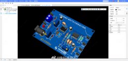
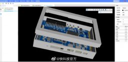
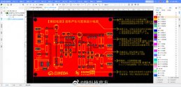
I appreciate your posts, but could you translate what you write into English? This is an English language forum after all.Hôm nay, Tongxin UOS chính thức công bố Jiali Chuang EDA chính thức ra mắt trên kho ứng dụng Tongxin, phần mềm do người Trung Quốc phát triển hoàn toàn độc lập.
This is a patent and design of a LPP EUV Lithograph. Not sure if a prototype has been manufactured and all parts tested.Does this imply that China has a prototype LPP EUV machine up and running? 30kW, 2 pulses per second and 50,000 drops/second?
If the prototype LPP EUVL has been manufactured and a MOPA CO2 Drive Laser of 30KW has been developed and produced, then this is a huge achievement for China.
I mentioned last year that China had already developed a MOPA CO2 Drive Laser of 10KW and was close to developing a 20KW plus MOPA CO2 Drive Laser. It is quite likely that they have sucessfully developed the 30KW MOPA CO2 Drive Laser by now. China has a highly developed Laser manufacturing industry.
It should be noted that the Current Model ASML NXE 3400 Series EUVL Lithograph uses a 30KW MOPA CO2 Drive Laser to produce Source Power of 250W.
So if a prototype LPP EUVL with its 30KW Drive Laser and the Optics has been tested, this means that China is close to producing its own EUVL which is competitive with the current ASML EUVL.
sr, my bad.I appreciate your posts, but could you translate what you write into English? This is an English language forum after all.
Definitely the former. Could be a mix of the two, but we don't know for sure.The increase in value can be attributed to either, all chips are now more expensive, or China reduced import of lower-end chips significantly while increasing import of higher-end chips.
- Status
- Not open for further replies.


