Chinese semiconductor industry

Status
Not open for further replies.

tokenanalyst

Brigadier
Registered Member
Actually, I think EUVL is easier than the space station.
The problem with EUV is the extreme accuracy that everything has to be done, this is from the research that has been made in CIOMP

Shortwave Optics - Extremely Fine


The uproar of the "ZTE Incident" has brought people's attention to the key components of the "chip", which seems to be inconspicuous but affects the whole body. A series of high-end equipment involved in chip preparation has become more and more important, and the most important of these is the lithography machine. The lithography projection objective is one of the core components of the lithography machine, and its design and manufacture represent the highest level of contemporary precision optics and precision machinery.

The difficulty of lithography objectives is concentrated in two words - "precision" .


Taking the EUV lithography objective lens as an example, its optical system consists of 6 aspherical mirrors the size of a pot cover. These mirrors have extremely stringent surface shape accuracy requirements, coating requirements and support requirements. Give a few examples to see what kind of extreme precision is achieved!


l The surface shape of the reflector requires that the fluctuation degree of the surface should be much less than one nanometer, which is equivalent to that the fluctuation cannot exceed 0.5mm on such a large area in Jilin Province ;


l In addition, dozens or even hundreds of ultra-thin films should be coated on such a flat surface, and the surface shape error after coating is also better than 1 nanometer, which is equivalent to a uniform surface on such a large area in Jilin Province. Spread a sheet of thousand-layer cake, and the thickness deviation of the cake should be less than 0.5mm ;


l The tilt adjustment control between the mirrors should be at the sub-nanometer radian level, which is equivalent to controlling a beam of light directed at the moon 380 million meters away, and accurately positioning the beam on the moon within 10 centimeters.


Therefore, the design and manufacture of the lithographic projection objective represents the highest level of precision optics and precision machinery in equipment manufacturing, and is the most sophisticated and complex optical system that can be developed by human beings at present.

In June 2017 , the "Key Technology Research of Extreme Ultraviolet Lithography" undertaken by the State Key Laboratory of Applied Optics successfully passed the preliminary acceptance, and obtained EUV projection lithography 32nm exposure pattern for the first time in China, laying a solid foundation for China to truly master high-end microelectronics manufacturing technology. foundation.
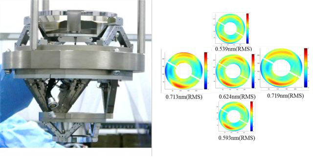
  

W020181026421762569854.png


  Fig. 3 EUV lithography objective (image source: research group) Fig. 4 Wave aberration distribution diagram of projection objective lens system (image source: research group)​

Please, Log in or Register to view URLs content!


As you can see the precision needed is just extreme. Another example is from the research in the Shanghai institute of fine optics and mechanics SIOM.

Representative results:

1. The extreme ultraviolet lithography wave aberration detection system developed as the technical leader has a 48 -hour wavefront long-term measurement repeatability of 0.1nmRMS , and a 38 -day wavefront long -term test repeatability of 0.24nmRMS .

Please, Log in or Register to view URLs content!

The precision of that instrument reached 0.1nm, that is like measuring an hydrogen atom for 48 hours and a silicon atom for a month without fail. The Chinese has done a great job but the task of developing such systems should not be underestimated whatever is LPP or SSMB, this are physics to the extreme.
 

coolgod

Colonel
Registered Member

Wanye Enterprise in-depth report: orders for integrated circuit equipment are nearly 1.1 billion, and the layout of semiconductor components continues to increase​


Highlights of the company: 1. Keystone has achieved full coverage of ion implanter integrated circuits, photovoltaics and AMOLED, and the first batch of commercialized equipment has been gradually delivered smoothly. Effective product transformation and market transformation, no domestic competitors, and an oligarchic position, the performance of this part is expected to accelerate in the later stage.
For some reason I read that news as Wayne enterprises, and I also read Keystone as Keysight. @_@
I was so lost so I had to google to see the connection and see if the equipment manufacturer was bought out by a new holding company named Wayne Enterprise.
 

tinrobert

Junior Member
Registered Member

ansy1968

Brigadier
Registered Member
This seems important, but I don't know enough about chips and fabs to be certain:


Link to original source:
Please, Log in or Register to view URLs content!
Bro SCMP had pick it up, I know TSMC and Samsung had been mass producing 7nm chip BUT Intel? Well success had many fathers and failure is an orphan, like the Indians the US want to be compared and associated themselves with winners...lol

And SMIC secret ingredients is a person named Liang Mong Song.

TechInsights noted that SMIC took only two years to reach 7-nm capability even “without access to the most advanced Western equipment and technologies”. By comparison, TSMC and Samsung took three and five years, respectively, to reach the same level.

China’s top chip maker SMIC achieves 7-nm tech breakthrough on par with Intel, TSMC and Samsung, analysts say​

  • SMIC took two years to achieve the leap from 14-nm to 7-nm, faster than TSMC and Samsung, TechInsights said
  • Experts said it is technically possible for SMIC to produce 7-nm chips even without the most advanced production equipment

Please, Log in or Register to view URLs content!


Please, Log in or Register to view URLs content!
in Beijing
+ FOLLOW
Published: 10:00pm, 29 Aug, 2022

A Chinese flag near the Semiconductor Manufacturing International Corp (SMIC) headquarters in Shanghai, China. Photo: Bloomberg

A Chinese flag near the Semiconductor Manufacturing International Corp (SMIC) headquarters in Shanghai, China. Photo: Bloomberg
A Canada-based research firm has doubled down on its earlier conclusion that China’s top chip maker
Please, Log in or Register to view URLs content!
had made a key technological breakthrough that puts it on a par with industry giants.
TechInsights, which
Please, Log in or Register to view URLs content!
that SMIC had begun using the 7-nanometre process to produce semiconductors after inspecting a sample chip extracted from a cryptocurrency mining machine, published a follow-up report on Monday.
Analysts said in the updated research note that SMIC had indeed achieved technological maturity, as measured by “standard cells” – the basic building blocks in logic chipset designs – that can rival the world’s leading foundries, such as
Please, Log in or Register to view URLs content!
and
Please, Log in or Register to view URLs content!
.
SMIC, which is on a US trade black list and facing additional restrictions on the import of advanced equipment, declined to comment on the findings when reached by the Post. The Hong Kong-listed company’s financial statements do not contain any mention of 7-nm grade technology.

China condemns new US law aimed at boosting domestic semiconductor manufacturing​

The technological progress of SMIC is being keenly watched by industry analysts, who are keen to find out if sanctions imposed by the US and its allies will crush China’s goal of achieving semiconductor self-sufficiency, a major point of rivalry between the two nations.


China’s push to catch up on chip technology faces strong headwinds after the White House signed the
Please, Log in or Register to view URLs content!
into law, with the aim of deterring TSMC, Samsung, Intel and others from investing in advanced manufacturing, including 7-nm process technology or newer, in mainland China.
Washington is also lobbying the Dutch government to block ASML Holdings, which has a monopoly position in the production of advanced chip-making machines, from selling to mainland Chinese foundries, including SMIC.

TechInsights noted that SMIC took only two years to reach 7-nm capability even “without access to the most advanced Western equipment and technologies”. By comparison, TSMC and Samsung took three and five years, respectively, to reach the same level.
The Ottawa-based firm in July reverse-engineered a MinerVA bitcoin mining processor made by SMIC and concluded that the Chinese chip maker had achieved a technological breakthrough despite having no access to the industry’s most advanced extreme ultraviolet lithography systems from ASML.
Pedestrians walk past the SMIC headquarters in Shanghai. Photo: Bloomberg


Analysts and professionals said it is technically possible for SMIC to produce 7-nm chips with existing deep ultraviolet systems under
Please, Log in or Register to view URLs content!
, a semiconductor industry veteran who was previously an executive at TSMC.

The latest findings by TechInsights suggest that SMIC has implemented many process integration choices deployed by TSMC, as “there are many similarities in process technologies, designs and innovations between SMIC’s 7-nm and TSMC’s 7-nm”.

SMIC was added to the US Commerce Department’s so-called Entity List in December 2020. At the time, the company said the sanctions, which prevent it from buying US-origin technologies, would hinder its development of technology below 10-nm, which is used in making advanced processors for smartphones and computers.

Since then, SMIC has shifted its focus to mature 28-nm technology. The company said over the weekend that it was
Please, Log in or Register to view URLs content!
in developing a new 12-inch wafer production line in the northern industrial hub of
Please, Log in or Register to view URLs content!
.
 

Nutrient

Junior Member
Registered Member
Chip power consumption is insignificant compared to the power required to do things like fly, drive, lift a heavy gun, operate a radar, etc. Aircraft produce more power than a power plant.
For large machines like tanks, yes, the power the AI would consume would be an insignificant fraction of the total power. However, I wasn't thinking large. Far cheaper than tanks would be swarms of tiny autonomous drones, each carrying flechettes loaded with neurotoxin. If you released a hundred thousand of them, they would totally destroy any human infantry. Now imagine releasing them inside a city: urban warfare would be almost easy.

Of course, such drones would need AIs more advanced than anything any country currently has, to operate in complex, real-world environments -- and to distinguish friend from foe. The AI would consume a significant fraction of such a drone's total power.

For example, consider a drone the size of a
Please, Log in or Register to view URLs content!
, which for many people is the state of the art today for small drones, or close to it. It's nowhere near autonomous, but let's ignore this. The drone's battery capacity is 3.8 Ah, it runs at 11.4 volts, and it flies for 27 minutes max. Thus it consumes 96 watts while flying. Now even a monster CPU like an Intel Core i9 10900K would be barely enough to run the simplest, most primitive AI -- and yet this monster will consume 250 watts TDP, several times the Mavic's total power. This is not "insignificant".

Thus even EUV lithography may not be enough, though breakthroughs in AI could happen to reduce the necessary computation load. If these breakthroughs don't happen, my hopes are on the neuromorphic chips, which are at least partly analog and therefore consume less power than fully digital devices. Analog circuits are less precise, but AI's neural nets are rather fuzzy anyway.
 
Last edited:

FairAndUnbiased

Brigadier
Registered Member
For large machines like tanks, yes, the power the AI would consume would be an insignificant fraction of the total power. However, I wasn't thinking large. Far cheaper than tanks would be swarms of tiny autonomous drones, each carrying flechettes loaded with neurotoxin. If you released a hundred thousand of them, they would totally destroy any human infantry. Now imagine releasing them inside a city: urban warfare would be almost easy.

Of course, such drones would need AIs more advanced than anything any country currently has, to operate in complex, real-world environments -- and to distinguish friend from foe. The AI would consume a significant fraction of such a drone's total power.

For example, consider a drone the size of a
Please, Log in or Register to view URLs content!
, which for many people is the state of the art today for small drones, or close to it. It's nowhere near autonomous, but let's ignore this. The drone's battery capacity is 3.8 Ah, it runs at 11.4 volts, and it flies for 27 minutes max. Thus it consumes 96 watts while flying. Now even a monster CPU like an Intel Core i9 10900K would be barely enough to run the simplest, most primitive AI -- and yet this monster will consume 250 watts TDP, several times the Mavic's total power. This is not "insignificant".

Thus even EUV lithography may not be enough, though breakthroughs in AI could happen to reduce the necessary computation load. If these breakthroughs don't happen, my hopes are on the neuromorphic chips, which are at least partly analog and therefore consume less power than fully digital devices. Analog circuits are less precise, but AI's neural nets are rather fuzzy anyway.
At 7 nm node already half the transistors are unused due to thermal overload and at 5 nm 80% the entire chip is unpowered.

Please, Log in or Register to view URLs content!

So mere die shrinks cannot solve the fundamental problem of thermal loading and cannot make fantasy AI weapons. You'd need a new paradigm like chip integrated cooling and much more efficient software. I don't know much about software but chip integrated cooling still doesn't solve the total power problem because you now need a heat pump to exhaust the heat generated and overall power consumption still increases.
 

PopularScience

Junior Member
Registered Member
Now the question to be ask is what next? Can we expect another miracle from Liang Mong Song and SMIC with a 5nm chip? IF we go by the development pattern, maybe we can expect a 5nm N+3 (DUV) in 2023 using NXT 2050i IF the said DUVL can deliver as advertised.
Liang Mong Song should be awarded National Technology Breakthrough of the Year prize.
 
Status
Not open for further replies.
Top