Chinese semiconductor industry

Status
Not open for further replies.

Nutrient

Junior Member
Registered Member
A followup to ....
So the US will loudly announce the success of the Chip 4 alliance -- see, even the South Koreans are on board -- and not say that most of the key provisions have been gutted. Yoon would probably love to kiss Uncle Sam's smelly feet, but his country's semiconductor companies are gagging on the odor. I see the exemptions as a face-saving way for Yoon to join Chip 4 without suffering much.
I advise Yoon to be extremely careful about joining Chip 4, even with exemptions. If he does sign the Chip 4 treaty, the Americans could simply ignore the exemptions and force the Koreans to obey every word of the treaty, especially the anti-China sanctions. Yes, that would be a very dirty thing for the Americans to do. But as we all know, the US is non-agreement-capable. If the US chooses to play dirty, what could Yoon do? Nothing.
 

tokenanalyst

Brigadier
Registered Member
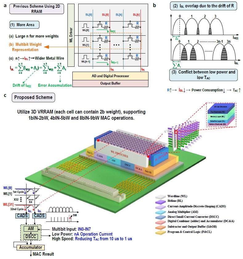
With the advancement of chip manufacturing, the process is gradually approaching the physical limit, and the development of deep neural networks has increased the amount of computation and parameters exponentially. The application of resistive memory to large-scale neural networks faces several challenges: 1 ) Due to convolution The increasing number of neural network weights makes the area overhead of resistive memory larger and larger; 2 ) For multi-valued large-scale resistive memory arrays, when the number of resistive units participating in the multiply-accumulate calculation is large, due to the large number of resistive units The accumulation of errors caused by conductance drift is more serious; 3 ) The three-dimensional resistive memory array is more difficult to manufacture, making it difficult to realize the co-design of resistive elements and circuits.

  In response to the above problems, the team of Academician Liu Ming from the Key Laboratory of the Institute of Microelectronics has developed an in-memory computing macrochip based on three-dimensional resistive memory. The researchers combined the multi -level self-selective ( MLSS ) three-dimensional vertical resistive memory with the anti-drift multi-bit analog input weight multiplication ( ADINWM ) scheme to achieve high-density computing; Based on the analog input weight multiplication scheme, a current amplitude discrete shaping ( CADS ) circuit is proposed to increase the sensing margin ( SM ) of the readout current for subsequent accurate analog multiplication calculation, which solves the problem due to the three-dimensional resistive memory array unit. Unrecoverable read current distortion caused by conductance fluctuation in traditional parallel word line input in-situ multiply-accumulate scheme; three-dimensional vertical resistive memory array using nA -level operating current to reduce system power consumption, while introducing switching follower with gate precharge ( GPSF ) analog multiplier and direct low-current analog-to-digital converter to reduce delay. When the input, weight and output data are 8 -bit, 9 -bit and 22 -bit respectively, the bit density is 58.2 bit/μm –2 and the energy efficiency is 8.32 TOPS/W . Provides more accurate brain MRI edge detection and higher inference accuracy on the CIFAR-10 dataset than traditional methods.

  The above research results were published online in the international top journal " Nature Electronics " in the field of electronics under the title of "A Computing-in-memory macro with three dimensional resistive random-access memory" , which realized the realization of the microelectronics research center of the Chinese Academy of Sciences. Zero breakthrough in the sub-journal of Nature . Dr. Huo Qiang from the Institute of Microelectronics is the first author, Yang Yiming from the Beijing Institute of Technology is the co-first author, and researcher Zhang Feng from the Institute of Microelectronics and associate professor Wang Xinghua from the Beijing Institute of Technology are the co-corresponding authors.

W020220829499965676889.png


  Figure 1. Challenges of applying 2D RRAM to large 3D CNNs and the proposed 3D computing scheme. a . More weights, multi-bit weight representation, and wider metal lines introduce more design challenges . b . The challenge of readout current is overlap and the conflict between low power consumption and low latency. c . High-precision non-volatile in-memory computing scheme based on MLSS 3D VRRAM . The ADINWM scheme of CADS circuit can effectively alleviate the current overlap caused by the traditional PWIVMM scheme and improve the inference accuracy. The implementation of CIM macros based on integrated 3D VRRAM chips expounds a complete solution for performing CNN edge computing.


Please, Log in or Register to view URLs content!
 

Nutrient

Junior Member
Registered Member
I think that after Chip 4 alliance, China has to put localized EUV machine development on super high priority lane, eventually fully in parallel with DUV. It is quite fascinating that a single machine has so much power!
Yes, the potential military applications of advanced AI would require EUVL. The Americans haven't said so, but I suspect that military reasons were the main drivers for preventing China from obtaining state-of-the-art lithography machines. So, just like the space station, the Middle Kingdom will make those machines. Actually, I think EUVL is easier than the space station.
 

tokenanalyst

Brigadier
Registered Member
Yes, the potential military applications of advanced AI would require EUVL
No necessary, like the auto industry military applications care more on reliability than the latest node. You don't want that chip to fail in a critical mission. Of course having smaller transistors gates mean less power, that is good news for developing thinner more battery lasting smartphones but someone can get the same or more raw power with more mature techniques if power consumption is not a concern but reliability is. Just think that the Chinese manage to develop two exaflops supercomputers using older mature IC nodes by optimizing the architecture.

Please, Log in or Register to view URLs content!

I think the driving force of AI will be geometrical scaling (Advance Packaging) and advanced deposition techniques (ALD and Epitaxial growth) rather than dimensional scaling . Geometrical scaling will be like how brain grows, neurons in a brain do not become smaller to accommodate more neurons, the package just scale geometrical, the package growth bigger and the brain folds into itself, this is a cheap process for nature. So I guess once the thermal and design issues with advanced 3D packaging are solved geometrical scaling will probably overtake dimensional scaling some areas like AI.

Please, Log in or Register to view URLs content!

But let suppose you are still hell bent of having the smallest transistor ever, I have news, it may be to keep dimensionally scaling possible without needing EUV. But what about yield? whatever the yield may be, for military applications, they usually don't care as long they get what they want.

Please, Log in or Register to view URLs content!

Please, Log in or Register to view URLs content!
 

tokenanalyst

Brigadier
Registered Member

Addressable WAT Test of Domestic Semitronix Tester​


Traditional WAT test is executed on a series of testkeys which is located in the scribe line of wafers. A transparent disadvantage of this kind of test is large amount of test time and limited number of DUT(device under test). So a different kind of WAT test is urgently needed, which combines the advantages of testing efficiency and accuracy. This paper will introduce a novel WAT test, it adopts parallel test based on specially designed testkey structure. What's more, domestic Semitronix tester is able to conduct this test, huge amount of time is saved, and testing accuracy is guaranteed.

Shanghai Huali Integrated Circuit Manufacturing Co., LTD

Please, Log in or Register to view URLs content!

Please, Log in or Register to view URLs content!

1661813847219.png
 

Nutrient

Junior Member
Registered Member
[EUVL not necessary for AI], like the auto industry military applications care more on reliability than the latest node. You don't want that chip to fail in a critical mission. Of course having smaller transistors gates mean less power, that is good news for developing thinner more battery lasting smartphones but someone can get the same or more raw power with more mature techniques if power consumption is not a concern but reliability is. Just think that the Chinese manage to develop two exaflops supercomputers using older mature IC nodes by optimizing the architecture.
Some of the potentially best (and deadliest) military applications of AI are for machines that operate autonomously, like drones and robots. These machines won't be plugged into large power plants. The reduction of their CPU's power consumption will therefore be critical to allow the necessary heavy computation, which means small geometries will be vital, which means EUV lithography (or maybe something even better, such as carbon nanotubes).

The neuromorphic chips look promising, but I don't know if they will ever reach their potential, or if they do, whether they will ever need EUVL. Time will tell.


Please, Log in or Register to view URLs content!

Please, Log in or Register to view URLs content!
Very interesting, thanks.
 
Last edited:

FairAndUnbiased

Brigadier
Registered Member
Some of the potentially best (and deadliest) military applications of AI are for machines that operate autonomously, like drones and robots. These machines won't be plugged into large power plants. The reduction of their CPU's power consumption will therefore be critical to allow the necessary heavy computation, which means small geometries will be vital, which means EUV lithography (or maybe something even better, such as carbon nanotubes).

The neuromorphic chips look promising, but I don't know if they will ever reach their potential, or if they do, whether they will ever need EUVL. Time will tell.


Very interesting, thanks.
military vehicles uses fossil fuel engines because they have incredibly high energy density, much moreso than batteries. as an example a
Please, Log in or Register to view URLs content!
mechanical power from small <2.0 L engines.
Please, Log in or Register to view URLs content!
- an embedded computer that can be used for robots, but mostly used to teach embedded programming, uses
Please, Log in or Register to view URLs content!
SoC fabbed on 40 nm. It consumes power in the ~5 W range. BCM2837 isn't a simple MCU, chip, it is an actual SoC with ethernet, USB, Wifi, CPU, GPU, etc. You can actually run a full Linux operating system on it.

Chip power consumption is insignificant compared to the power required to do things like fly, drive, lift a heavy gun, operate a radar, etc. Aircraft produce more power than a power plant.
Please, Log in or Register to view URLs content!
, enough to power a small town, and military aircraft have at least 1 engine just to be able to take off and fly around.

As for what a Raspberry Pi 3 can do,
Please, Log in or Register to view URLs content!
. It is faster than the
Please, Log in or Register to view URLs content!
If you need higher performance, just stack more chips in a package. The #1 priority for military products is environmental hardening.
 

antiterror13

Brigadier
Yes, the potential military applications of advanced AI would require EUVL. The Americans haven't said so, but I suspect that military reasons were the main drivers for preventing China from obtaining state-of-the-art lithography machines. So, just like the space station, the Middle Kingdom will make those machines. Actually, I think EUVL is easier than the space station.

I believe so that EUV is surely easier than space station,

Even GPS/Compass is more difficult that EUV ... I think so

but honestly I can't back up my claim here ..... sorry

Can the Dutch make a space station? BIG NO, not even the whole EU

Can the Dutch make GPS system? BIG NO, even the whole EU is behind China now
 

Canton_pop

Junior Member
Registered Member
Too much is made out of the phones.

In the end, that is all the Americans can claim to accomplished, in the war against Huawei 5G.

Huawei sold less phones. The trade off there, is that the UAE cancelled their 23 billion dollar contract for F-35. Huawei lost about 28 billion in sales mainly over the phones last year. What a trade off that is. Cell phones for F-35.

-------------- --------------

Sometimes, when the fight is that intense, we forget about longer term strategic thoughts/plans.

For example, this energy crisis in Europe. Before the Russian invasion of Ukraine, they were happily enjoying cheap energy. After the special military operation, they are in crisis. The former was better than the latter. They were working together for mutual benefit. Now they are divided. Got to wonder about this. Was it European stupidity or American ingenious, that allowed the continent to be divided & conquered? That is all that is. Who really gives a shit about the Ukraine.

What started as a US government war against Huawei 5G, has turned into a broader technology war between the United States and China itself.

Wars have a tendency to expand.

This war the United States basically have one big advantage, the only point of leverage over China, which is IC equipment.

1. Whether this advantage in IC equipment can achieve anything is debatable. Huawei beat the Americans in building out 5G because they had a stockpile of chips.

2. The future challenges in this tech war will be more intense for the Americans, and really, not sure if they can handle that. They could not handle this Huawei 5G war very well, to the point they stopped talking about it.

Strategically speaking, I thought this tech war was really dumb.

If you're going into a war, with only one real point of strength, then what kind of advantage do you have, really?

Then to further complicate it, that only point of strength, needs those so-called allies, who did not even want to met Pelosi when she arrived on her broomstick.

Decoupling, is just the euphemism for tech war here.

It won't succeed. It does not have a chance.

Remember how Huawei beat the semiconductor chip supply ban imposed on them?

They gave TSMC a big order to stockpile chips!

Then next of course, China builds out its national 5G network.

That was the only thing required to beat the Americans now, which is a stockpile of chips.

Later, just improve domestic IC capability. They have made progress.

In the end, that stockpiling of chips, was a key factor. Huawei beat the Americans at that game of building out 5G, with a stockpile. That's it.

Now the Americans, they are still playing the same game, with the same playbook, calling the same plays. Guess we can expect Chinese companies will start stockpiling chips again, until domestic IC lines come online.

The Americans seem particularly desperate. Notice how we never hear a peep about the Huawei stockpile of chips anymore? Simply because China built out its 5G network.

That is all it took for Huawei to beat the Americans. A stockpile of chips. Then improving domestic IC capability.

This does not appear that the Americans were beat. They were crushed.

Rumours have it that Huawei itself is coming out with a new chip soon. How long has this Huawei 5G versus US government war been going on? And Huawei is coming out with a new chip?

Hey, what can we say? Just wish that Chip-4 alliance the best of luck, long live the Chip-4 alliance.

:D
Chip 4 and all the sanctions by US is the best push factor for Made in China 2025 than what Xi can ever dream of.
 

tokenanalyst

Brigadier
Registered Member

Wanye Enterprise in-depth report: orders for integrated circuit equipment are nearly 1.1 billion, and the layout of semiconductor components continues to increase​


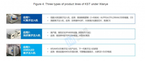
Highlights of the company: 1. Keystone has achieved full coverage of ion implanter integrated circuits, photovoltaics and AMOLED, and the first batch of commercialized equipment has been gradually delivered smoothly. Effective product transformation and market transformation, no domestic competitors, and an oligarchic position, the performance of this part is expected to accelerate in the later stage.

1661821795209.png

2. Jiaxin Semiconductor's product planning ideas are clear, front-end equipment diversified capacity construction, and front-end integrated equipment delivery plan, covering etching machines, thin film deposition equipment, rapid heat treatment equipment, etc. After its establishment, it has over 340 million orders in hand Yuan, well-known experts and industry resources are blessed, and the market prospect is bright.

3. Zhejiang Compart Systems, which mainly focuses on precision components in the field of flow control. Its products cover flow control components, components, seals, gas rod assemblies, mass flow controllers (MFC), etc. of semiconductor equipment, and have been supplied for many years. The mature experience of the world's leading semiconductor equipment factories helps domestic semiconductor equipment manufacturers to rapidly promote the localization of core components.

4. The investment amount of the semiconductor industry will not be affected by the international economic situation and the relationship between major powers, and its development will be a special development path independent of the development of the world economy and trade. The development of domestic semiconductor equipment and materials will be the same as the development of new energy vehicles, which is a steady and unstoppable historical trend.

Since 2022, Wanye has received orders of nearly 1.1 billion yuan for integrated circuit equipment. Among them, Keystone H1 has received orders of more than 750 million yuan for multiple ion implanters from 3 customers, and the business has officially entered a period of heavy volume. Up to now, a variety of IC ion implanters developed and manufactured by Keystone, including low-energy large-beam ion implanters, low-energy large-beam heavy metal ion implanters, low-energy large-beam ultra-low temperature ion implanters and high-energy ion implanters, have all passed Validation and acceptance of 12-inch mainstream fab customers.

At present, the ion implanter of Keystone, a subsidiary of Wanye Enterprise, has been supplied to mainstream 12-inch wafer fabs in China and has become its strategic supplier. On the premise of the complete release of Keystone's production capacity, benefiting from the recognition of bulk purchasing strategic suppliers recognized by domestic mainstream customers, and benefiting from the good partnership with world-renowned semiconductor industry experts, Wanye will make domestic production of semiconductor front-end equipment. Under the wave of chemicalization, the industry pattern of ion implanter has formed a unique domestic industry. The growth space of ion implanter orders in the next 3-5 years will come from SMIC, JTA Semiconductor, Hua Hong Semiconductor, and Silan Microelectronics. , China Resources Micro, Changjiang Storage, Changxin Storage, Yuexin and other manufacturers' capacity expansion.


Please, Log in or Register to view URLs content!
 
Status
Not open for further replies.
Top