The Institute of Microelectronics, Chinese Academy of Sciences and Huawei HiSilicon have made progress in the research of spin-orbit moment magnetic tunnel junction devices without external magnetic field writing
The vertical spin-orbit moment magnetic tunnel junction device (SOT-MTJ) is the core unit of a new generation of magnetic random access memory technology. It has the characteristics of non-volatile, high speed, low power consumption, long read and write life, etc. Non-volatile magnetic storage technology. However, vertical SOT-MTJ devices require external magnetic field assistance to achieve directional writing.
The vertical spin-orbit moment magnetic tunnel junction device (SOT-MTJ) is the core unit of a new generation of magnetic random access memory technology. It has the characteristics of non-volatile, high speed, low power consumption, long read and write life, etc. Non-volatile magnetic storage technology. However, vertical SOT-MTJ devices require external magnetic field assistance to achieve directional writing. The introduction of an external magnetic field can lead to additional power consumption, area consumption, and can lead to problems such as crosstalk. How to realize directional high-speed writing SOT-MTJ nanodevices without external magnetic field is still a big challenge.
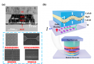
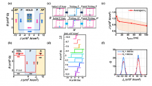
Recently, the researcher Luo Jun's team of the Integrated Circuit Leading Process R&D Center of the Institute of Microelectronics, Chinese Academy of Sciences cooperated with the Huawei HiSilicon team to jointly develop the back-end integration process of SOT-MTJ on the center's 8-inch CMOS platform, achieving a pitch of ≤360 nm, junction diameter ≤140 nm, TMR higher than 118%, and thermal stability coefficient Δ up to 118 tunnel junction arrays (Figure 1). The R&D team designed a tunnel junction thin film structure with strong interlayer coupling, and used the Joule heat generated by the writing current to control the coupling strength of the tunnel junction to achieve the characteristic curve of unipolar current writing (Figure 2(a)). Unlike conventional tunnel junctions, the high and low resistance states of this tunnel junction depend on the magnitude of the current, not the direction of the current (Fig. 2(b)). This is due to the fact that the Joule heating generated by the current modulates the magnitude of the interlayer coupling field of the tunnel junction, thereby modulating the bias field of the SOT-MTJ, resulting in the writing of different resistance states (Fig. 2(c,d)). The device can achieve a write speed of up to 1 ns (Fig. 2(e)) and is able to operate stably in a high temperature environment of 100 °C. In addition, the electrical properties of different devices within the chip have good consistency (Fig. 2(f)). This research result proposes a feasible non-field-assisted writing SOT-MTJ scheme, and helps to achieve high-density field-free SOT-MTJ array integration, laying the foundation for a new generation of large-capacity SOT-MRAM.
Relevant research results were published in the journal
IEEE Electron Device Letters (IEEE EDL, 43, (2022) 709) under the title of "
Field-Free Deterministic Writing of Spin-Orbit Torque Magnetic Tunneling Junction by Unipolar Current ", and was selected as an editor's recommendation article . Yang Tengzhi, a doctoral student at the Institute of Microelectronics, is the first author, and researcher Luo Jun, associate researcher Yang Meiyin and Huawei Haisi Ye Li are the co-corresponding authors. This work was supported by relevant projects of the Ministry of Science and Technology, the National Natural Science Foundation of China and the Chinese Academy of Sciences.

Figure 1. (a) Cross-sectional TEM and partial process top view of the SOT-MTJ device. (b) Schematic illustration of the structure and principle of the SOT-MTJ device.

Figure 2. (a) Electrical writing characteristic curve of SOT-MTJ. (b) The relationship between the storage state of the SOT-MTJ and the write current density. (c) Schematic illustration of the magnetic properties of different writing operations. (d) Coercive field and bias field as a function of write current density. (e) Critical write current density versus write pulse width. (f) Statistical distribution of critical write current density for randomly sampled devices.


