Chinese semiconductor industry

Status
Not open for further replies.

european_guy

Junior Member
Registered Member
Deep analysis of the market from Credit Suisse Japan with a lot of interesting data:

Please, Log in or Register to view URLs content!

Just some few highlights:

- Demand is increasing in China for equipment used in the assembly of EV power modules,
with Huawei-linked projects the reported driver of demand. Insulated-gate bipolar
transistors (IGBTs) and other components are being sourced from US, European, and
Japanese producers. (page 8)

- CXMT expansion plan (page 37)

- YMTC has revised its 196-layer plans and is focusing on improving yields for the 128-layer
chip for the time being (page 49)

- China's YMTC already uses bonding technology, but among global
players, Kioxia plans to build a test line in 2023 (around 30K units in 2Q), followed by mass
production in 2024 and Samsung Electronics targets adoption of the technology in 2026 (page 50)

- NAND technology roadmap (page 50)

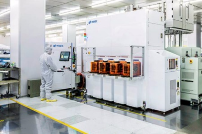
- Huawei plans to establish an in-house assembly line to supply the end-to-end-integrated
line being developed by Shaoxing-based SMIC spin-off Semiconductor Manufacturing
Electronics Corp (SMEC). (page 56)

- Chinese memory players CXMT and YMTC have pulled back on capital investment, but
YMTC has reportedly begun making inquiries about equipment since the June quarter (page 57)
 

tokenanalyst

Brigadier
Registered Member

Integrating traditional and innovative domestic EDA to fill the gap of RTL high-speed simulation​

Please, Log in or Register to view URLs content!


Jiweiwang reported that RTL verification in chip design has become one of the most critical links because of the most time-consuming and labor-intensive design. In order to improve the efficiency of RTL verification, help manufacturers to quickly bring products to the market. Shun Yao Electronic Technology (Shanghai) Co., Ltd. recently released the high-speed simulator ShunSim.

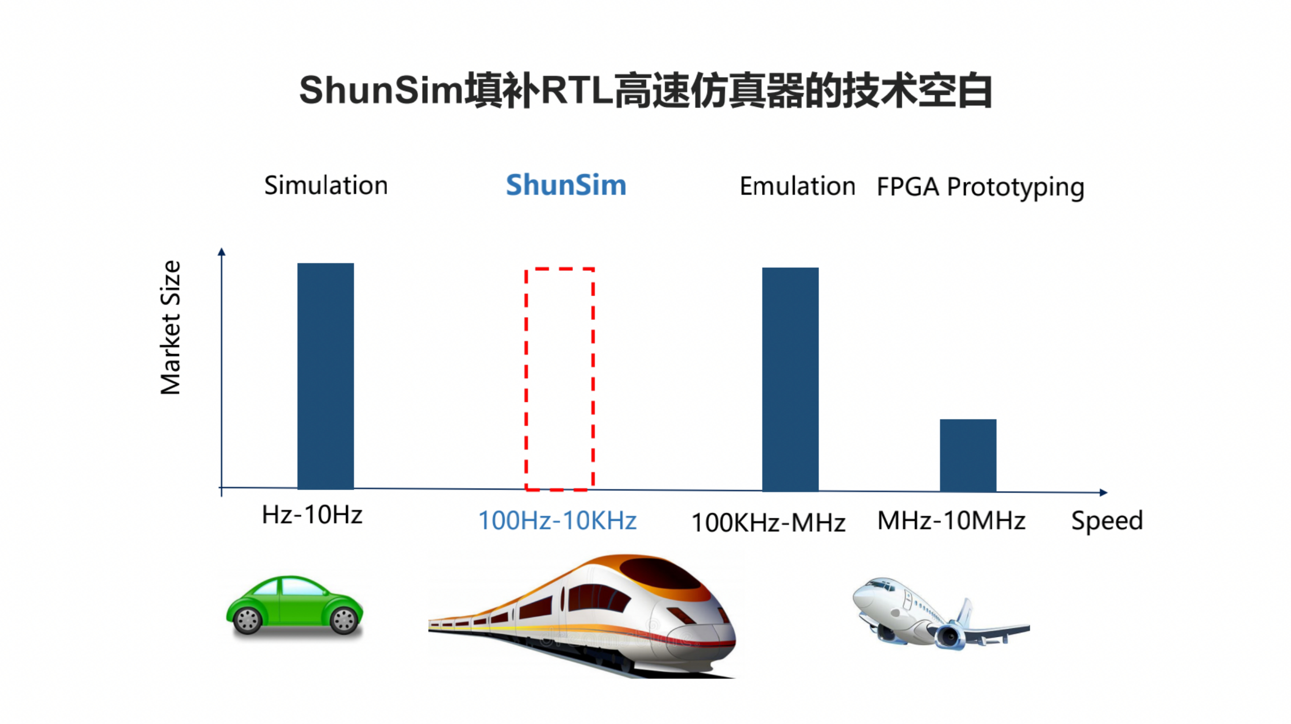
ShunSim fully considers the current design features and verification difficulties of VLSI, and its positioning is between Simulation, Emulation and FPGA Prototyping, filling the gap of verification technology.

1656937487421.png


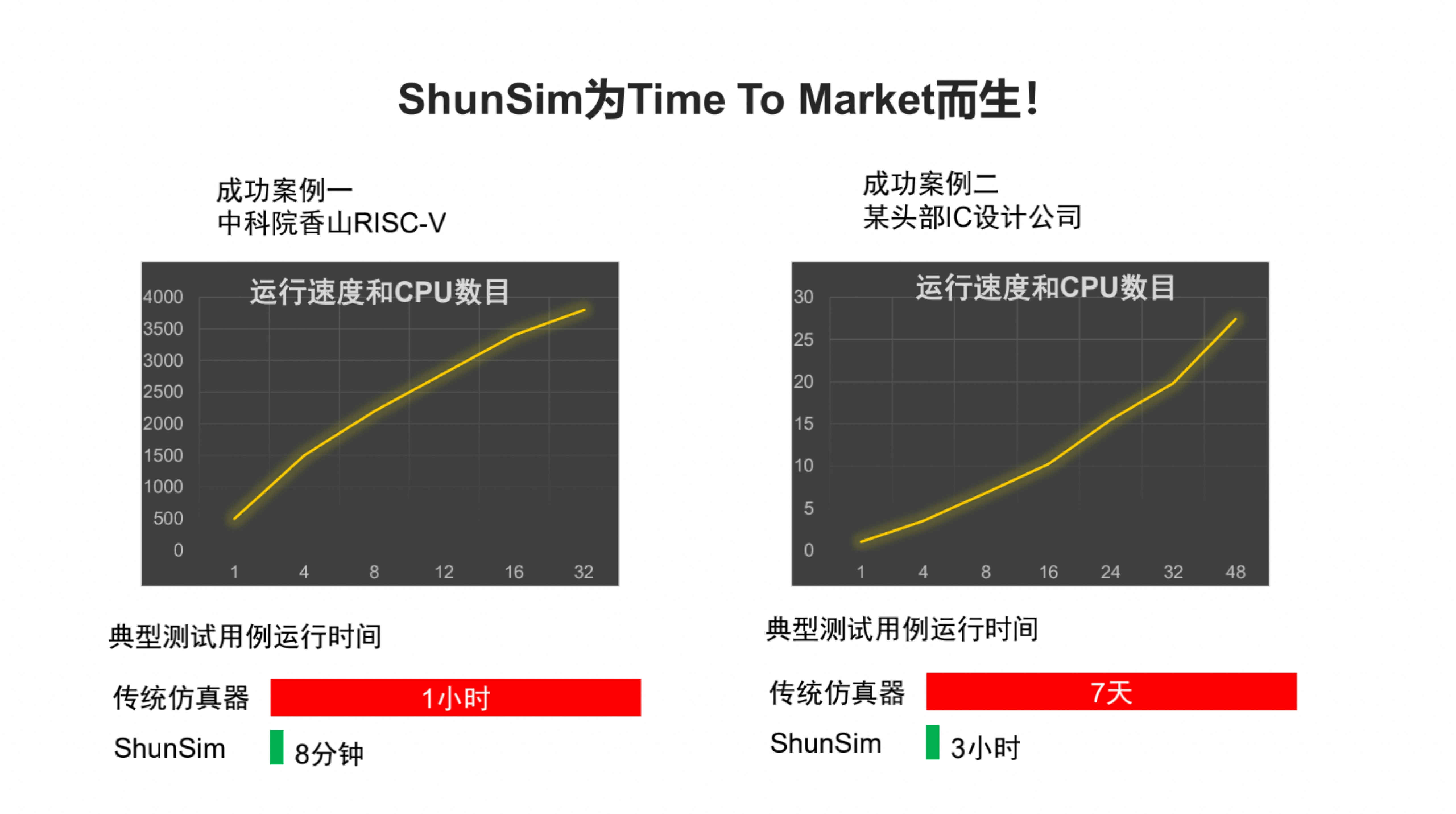
According to reports, ShunSim makes full use of and releases the multi-computing power of the server, and the speed can be 10-100 times higher than that of traditional simulators; built-in Verilator, a robust and safe simulation kernel verified by a large number of commercial cases; supports Verilog, System Verilog, C++, SystemC, etc. A variety of mainstream design and verification languages; with interactive mode, Force/Release, Save/Restore and other functions, flexible waveform generation function; native support for EDA verification IP series YaoVIP, which provides easier-to-use and more efficient complete chip function verification solution.

Fu Yong, founder and CEO of Verilator, said: "The kernel we use is an open-source emulator with 20 years of experience, and Verilator also provides support for the development of an open-source tool like Verilator."

"The core technology of Instant Light is to divide the large design into smaller designs, and then let these small designs run stably in the Verilator core." Fu Yong believes that this is the perfect fusion of tradition and innovation, which enables Instant Light to quickly launch satisfying Innovative products that the market needs.

16569375346127.png


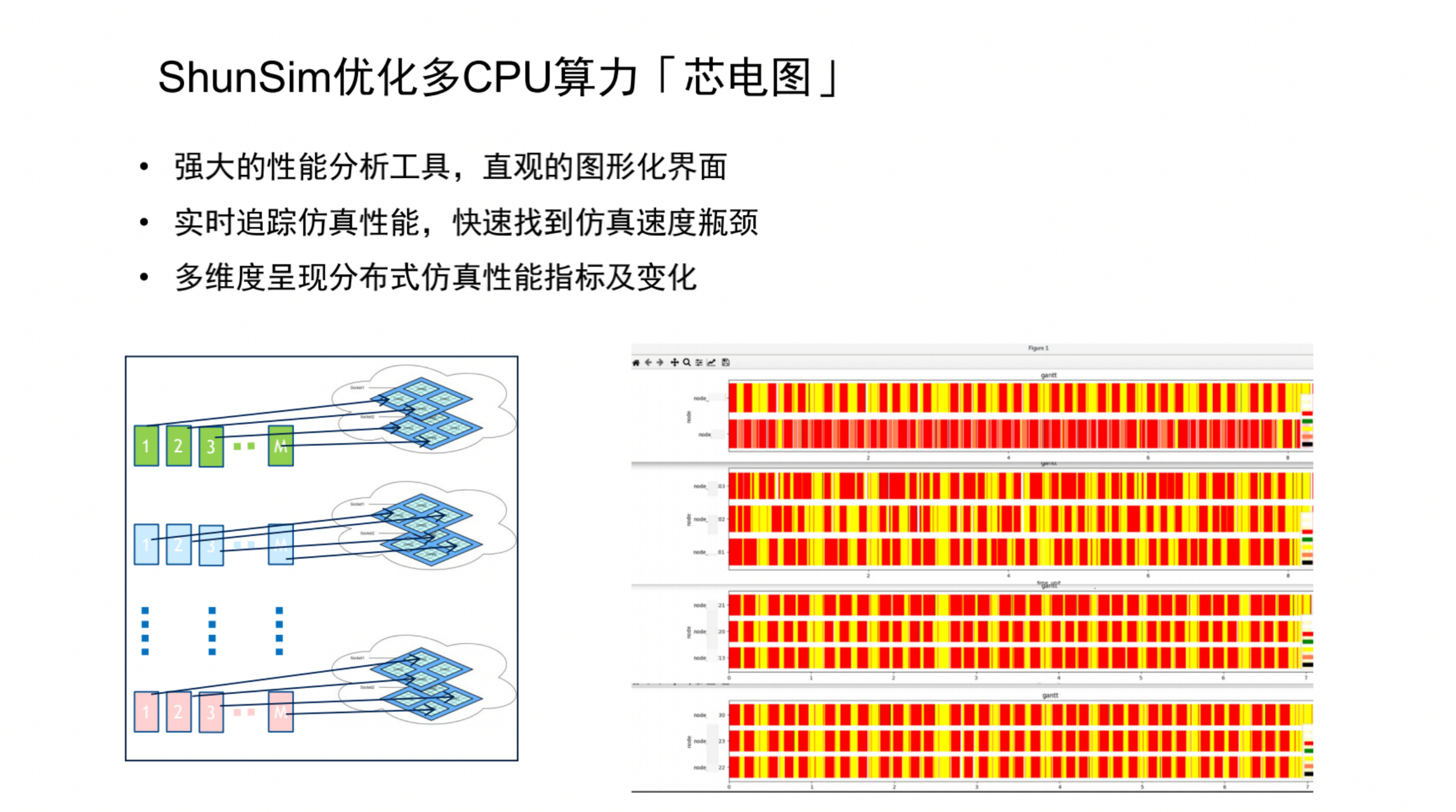
ShunSim can generate "electronograms" optimized for multi-CPU computing power. It has powerful performance analysis tools and an intuitive graphical interface; it has real-time tracking simulation performance, and quickly finds simulation speed bottlenecks; it can present distributed simulation performance indicators and changes in multiple dimensions.

Fu Yong explained the difference between ShunSim and several other verification methods: "When the design is at IP level, users will use Simulation, and when all designs are completed, they will consider using Emulation and FPGA Prototyping, ShunSim's The introduction is when the design scale is large enough that Simulation cannot run.”

Fu Yong made an image metaphor for ShunSim's market positioning: "The traditional emulator is a Xiaomi plus rifle in the hands of every verification engineer, and an emulator worth tens of millions is an ICBM in the hands of all IC design companies. ShunSim is more like a The sniper gun will more accurately target the market of this size and scale, and bring more benefits to customers with better cost performance.”

Because of its precise product positioning and excellent product quality, Shunyao won the first commercial order from a leading domestic enterprise at the beginning of half a year of establishment. In this regard, Fu Yong said: "The core of verification is to help IC manufacturers accelerate Time To Market, and ShunSim was born for this. We are very happy that Shunyao has been established for less than a year and has already been deployed by real customers, which is very helpful for us. The technical direction of the company is a very important recognition. At the same time, we still have a lot of R&D work behind us. We are willing to grow together with the leading IC design team. While serving customers well, we will polish and improve the overall verification scheme of Sunyao's characteristics as soon as possible. "

16569376445607.png


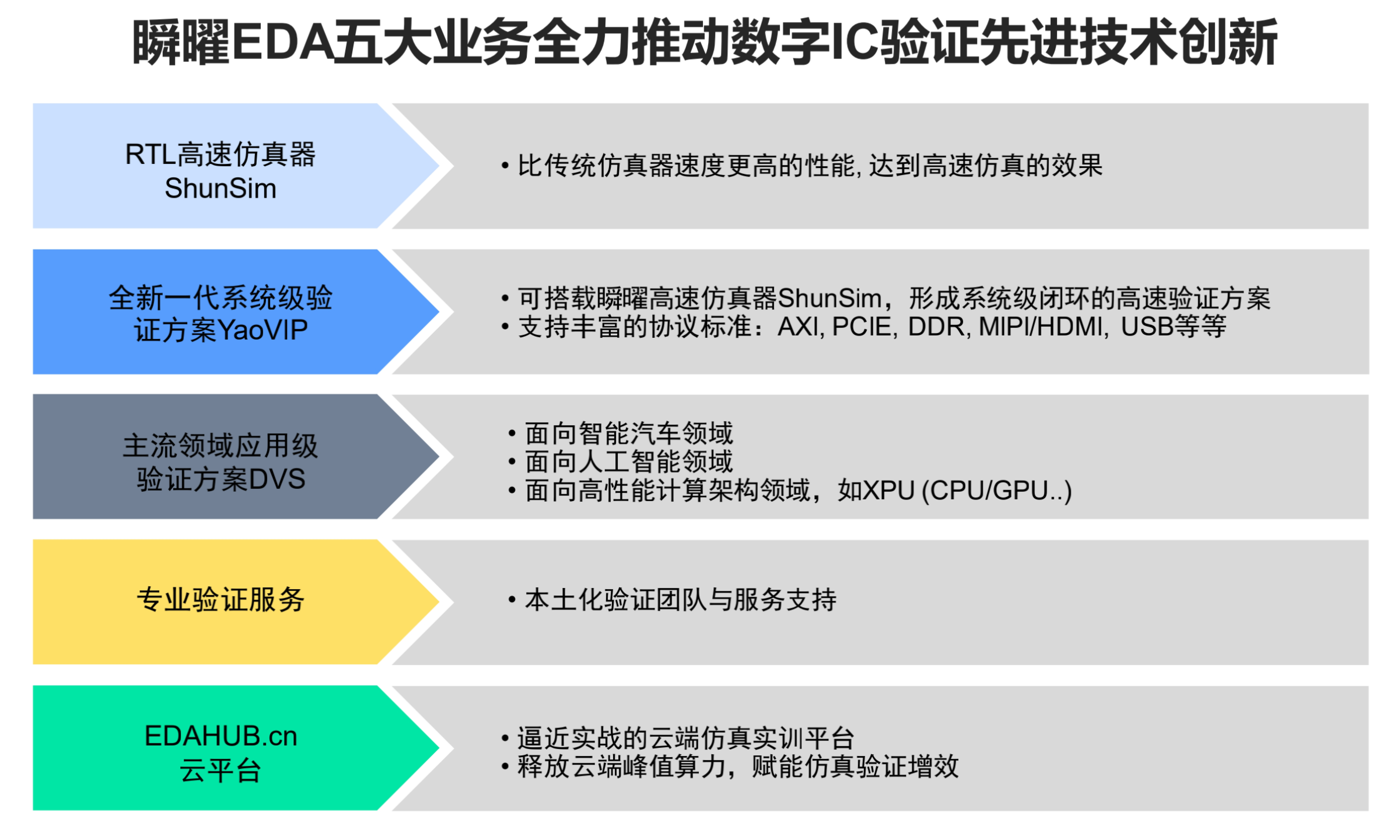
While providing high-speed simulator ShunSim for VLSI design manufacturers, Shunyao is also an important contributor to the internationally renowned open source tool Verilator and its recommended value-added service provider, which can provide a stable platform for small and medium-sized design manufacturers and university research institutes. simulation platform. In the future, Sunyao EDA will adhere to its commitment and original intention to the open source community, support the strategic development of open source EDA for a long time, and actively promote in-depth cooperation with domestic universities and research institutes.

16569377638564.png


Please, Log in or Register to view URLs content!
 

tokenanalyst

Brigadier
Registered Member
Ruili Scientific Instruments received 160 million yuan in financing


Recently, the company completed a round of capital increase, which directly injected more than 160 million yuan in cash . This round of capital increase was fully subscribed by some original shareholders. The funds raised in this round will be mainly used for product iterative research and development of optical film thickness measurement equipment and defect detection equipment, as well as new product research and development and production investment.

Since 2019, Reli has returned to the track of rapid development. The company's film thickness measurement, defect detection and optical critical dimension measurement equipment has been adopted by nearly 20 front-end semiconductor wafer manufacturing customers in China, and has passed large-scale mass production verification on different production process lines (accumulating hundreds of millions of It has been recognized by customers in terms of equipment stability and its ability to quickly respond to problems and solve problems. It has achieved remarkable results in helping production lines improve production efficiency, improve yield, and reduce equipment ownership costs. The 12 -inch film thickness measurement equipment TFX4000 series and the 12 -inch high-precision optical defect detection equipment WSD series for bright and dark fields launched in the past two years have been delivered to important domestic customers. Repeated sales orders.

After completing this round of financing, Reli will continue to deepen the market of integrated circuit chip production process testing equipment, further enrich the optical measurement and optical defect detection product series, and accelerate the development of optical film thickness measurement equipment, OCD measurement equipment, optical defect detection equipment. While the equipment and other products are iteratively updated, the development and application expansion of other optical testing equipment will be gradually opened, and efforts will be made to achieve full coverage of the application capabilities of similar equipment from international manufacturers as soon as possible, in order to achieve the goal of comprehensive replacement of localization of integrated circuit front-end process testing equipment as soon as possible. And work hard.
1656971123075.png

Please, Log in or Register to view URLs content!
 

tokenanalyst

Brigadier
Registered Member

Zhongwei Company: At present, the order of etching equipment is full​

Please, Log in or Register to view URLs content!


16569995616168.png


According to the news of the micro-net, recently, China Micro Company said in an institutional survey that the company's current localization rate of parts for etching equipment is about 60%, and the localization rate of parts for MOCVD equipment is about 80%.

At present, the company's products have entered the international supply chain, and the company has also built channels in major global markets. It has 6 overseas subsidiaries and 15 regional offices.

The company said that the company's etching equipment has been continuously improved in terms of process coverage, and the process of verification at the client is progressing well, and the current order situation is full.

In the early stage of the epidemic, Zhongwei Company made corresponding preparations: closed-loop production, logistics passes, customs clearance, etc. The company pays close attention to the situation of the epidemic and takes emergency measures for epidemic prevention, and earnestly implements the decision-making and deployment of the national and Shanghai government on epidemic prevention and control. With the support of relevant government departments and the company's efforts, the company's production and operation are basically normal.

With the development of the international advanced chip manufacturing process from 14nm to 10nm to 7nm, 5nm and more advanced processes, the current lithography machine is limited by the wavelength of light, it needs to combine etching and thin film equipment, using multiple template processes, The use of etching processes to achieve smaller dimensions further increases the importance of etching technology and related equipment.

In order to further enhance the technical advantages and market share of the company's etching equipment products, the measures taken by the company include but are not limited to:

(1) The company will continuously improve the R&D management mechanism and innovation incentive mechanism, and reward technical R&D personnel who have made outstanding contributions in technology R&D, product innovation, patent application, etc., to stimulate their enthusiasm for work.

(2) The company will continue to increase R&D investment, build a better R&D experiment environment, and provide an important foundation and guarantee for technological breakthroughs and product innovation.

(3) In terms of equipment research and development, while continuing to improve the performance of existing equipment, the company will segment products according to the different etching requirements of advanced logic chips and high-density storage DRAM and 3DNAND chips, and develop different hardware features to improve The etching performance of the products for different applications meets the needs of different customers. At the same time, the company will define the technical indicators and technical routes of the next-generation products according to the research and development needs of customers, and develop new products that can meet the needs of customers.

China Micro said that MOCVD equipment is currently widely used in the lighting and display markets. More importantly, the market expansion of Mini LED and Micro LED, and the development prospects of related markets are very promising. Important applications of MOCVD equipment also include power devices. Market institutions predict that by 2026, the global annual demand for more than 800 MOCVD equipment. China Micro has developed related products in three of these fields, and the company will continue to develop epitaxy equipment in the fields of lighting and display, including Mini LED, Micro LED, and power devices. The company expects to cover approximately 75% of the MOCVD equipment market. The future market space is very broad.

As a leading domestic etching equipment company, China Micro has obvious advantages in the entire process of localization of semiconductor equipment. The company has maintained large-scale and high-intensity R&D investment for a long time, but the company still has a big gap in the R&D layout and R&D scale of the international semiconductor equipment giants. The company will continue to increase the level of investment in technology research and development, and further narrow the gap in research and development with overseas giants in the same industry.
 

Overbom

Brigadier
Registered Member
US doesn't seem to know when and where to stop. It just keeps abusing its sanction powers. That's why it keeps shooting itself in the foot.
Please, Log in or Register to view URLs content!
That's basically a complete ban in my books. If it happens, time to go on a war-footing
American officials are lobbying their Dutch counterparts to bar ASML from selling some of its older deep ultraviolet lithography, or DUV, systems, the people said. These machines are a generation behind cutting-edge but still the most common method in making certain less-advanced chips required by cars, phones, computers and even robots.
 

FairAndUnbiased

Brigadier
Registered Member
Deep analysis of the market from Credit Suisse Japan with a lot of interesting data:

Please, Log in or Register to view URLs content!

Just some few highlights:

- Demand is increasing in China for equipment used in the assembly of EV power modules,
with Huawei-linked projects the reported driver of demand. Insulated-gate bipolar
transistors (IGBTs) and other components are being sourced from US, European, and
Japanese producers. (page 8)

- CXMT expansion plan (page 37)

- YMTC has revised its 196-layer plans and is focusing on improving yields for the 128-layer
chip for the time being (page 49)

- China's YMTC already uses bonding technology, but among global
players, Kioxia plans to build a test line in 2023 (around 30K units in 2Q), followed by mass
production in 2024 and Samsung Electronics targets adoption of the technology in 2026 (page 50)

- NAND technology roadmap (page 50)

- Huawei plans to establish an in-house assembly line to supply the end-to-end-integrated
line being developed by Shaoxing-based SMIC spin-off Semiconductor Manufacturing
Electronics Corp (SMEC). (page 56)

- Chinese memory players CXMT and YMTC have pulled back on capital investment, but
YMTC has reportedly begun making inquiries about equipment since the June quarter (page 57)
Wait didn't somebody here say wafer bonding I/O with memory array was a useless and expensive technology done as a cope by YMTC?
 

latenlazy

Brigadier
Wait didn't somebody here say wafer bonding I/O with memory array was a useless and expensive technology done as a cope by YMTC?
Anyone who says a technology is useless and expensive without qualifying the actual performance vs cost parameters and without addressing potential for improvement in technology or technique is more interested in pushing an opinion than doing good industry analysis. There are some people who are wedded to the view that only a reputable name can innovate validly, and yet these industries are moved almost entirely by improving on things that couldn’t be done or weren’t cost effective until someone manages to do them or make them cost effective.
 
Status
Not open for further replies.
Top