@Weaasel bro reading your post reminded me of @superdog , The Iconic quote " Getting a great sculpting knife doesn't mean you can immediately become a great sculptor." that saying is so true of China IC BUT the sculptor is getting better and is coordinating with his craftsman to create better tools.Remember that TSMC is only able to produce the most sophisticated IC chips in the world because it is provided with the tools and materials to do so, including EUV lithography machines, vapour deposition machines, and photoresists that are mostly imported. TSMC is a Taiwanese company and Taiwan is a defacto loyal vassal of the United States, so the United States will not object to its allies such as Japan, the Netherlands, any other EU country having their companies provide TSMC with equipment and materials necessary for it to produce such amazing chips. Even Chinese companies supply TSMC with vapour deposition and etching equipment.
An analogy for TSMC is that it is the best chef in the world, capable of cooking any meal very deliciously. But that chef doesn't produce his own ingredients, nor does he make the best cooking knives, pots, and pans that he cooks with. He purchases them from various suppliers.
Remember that Japan is capable of producing to high quality all equipment used in IC chip manufacturing except EUV lithography machines. Gigaphoton is a Japanese company that is capable of producing the power light source to vapourize tin droplets used in ASLM's EUV lithography machines, even though it is not the supplier of that light source. It is very plausible that if Japan committed itself politically it could acquire ASML's machines to produce 7 nm and below IC chips, establishing a company or bestowing one or more existing companies for that purpose. Additionally, Canon does possess nanoimprint lithography technology that can produce at nodes of less than 20 nm.
The main barrier to that, even given such political will, is not Japan's lack of technological capability but whether there is sufficiently a market for a new major Japanese entrant into it. China doesn't have that market barrier, since China is actually presently subject to a defacto partial embargo and has the domestic market to undertake import substitution on a highly dominant scale. China has already committed itself to such gradually heightened import substitution.
from @superdog circa April 27 2020.
Climbing the lithography tech tree requires decades of intensive research work, reacting after an embargo would be way too late.
The good news is that this has been in China's plans for decades.
The bad news is that the catch up game will still go on for many years, if not decades.
The saving grace is that if the semiconductor embargo intensifies, they will pour much more resources into this and catch up quicker.
is China's ASML, it has been working on lithography machines since the 10th 5-year plan (2001-2005). If you go to its website you can see its most recent lithography product (SSB600 series) supports ArF light source dry lithography. This was announced in 2016, and machines with similar specification are typically used for making chips with process nodes of 130-65nm.
The SSB600 series was not commercially successful and still depended on some important foreign components. It was more of a research milestone rather than a business one.
The current product being developed by SMEE is said to be the SSB800 series, which is an ArF light source immersed lithography machine. This was funded by the "28nm node immersive lithography machine" topic, under the "02 project" and the 13th 5-year plan (2016-2020). Expected delivery is 2021. It can also be expected that the machine will have less foreign dependency, as local upstream suppliers (Beijing Guowang Optical Tech, , Changchun Institute of Optics etc.) are providing key components such as the light source, the optical system, and the "dual wafer stage" design, all of which are sub-topics in the 02 project.
It is important to understand that one generation of lithography machine corresponds to multiple generations of chip process nodes. How far the machine can be pushed also depends on the technical know-how of the foundry. For example, SMIC owns the same model of ASML ArF immersed lithography machines that TSMC used to make 1st gen 7nm chips, but SMIC only just started 14nm production. Getting a great sculpting knife doesn't mean you can immediately become a great sculptor.
We don't know what is the process node limit of the SSB800 series. It is technically in the same generation of ASML's DUV machines that TSMC pushed up to 7nm, but that took the most advanced foundry and a much more mature lithography product line to achieve. My guesstimate is that for the SSB800, 28nm would be a good initial trial target (also required by the national plan), and 10-14nm should be within reach after some adjustment and improvement. 7nm is questionable, I think it depends on how long China will get stuck on DUV.
To go beyond 7nm, it is necessary up a generation and get EUV lithography machines. I heard they've made good progress in EUV light source (which is a key technical challenge), otherwise little is known about the progress of a domestic EUV machine. I don't expect to see it soon, but it is in their plan for sure.
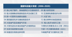
The difficulty to catch up in semiconductor manufactoring must not be underestimated, and China is one player that don't underestimate things. You know, the full name of the 02 project is "The project of manufacturing technology and complete sets of technology for very large scale IC's", but why do people call it the 02 project? Because it is considered the 2nd most important in all of China's 16 long term tech development projects.

