You are using an out of date browser. It may not display this or other websites correctly.
You should upgrade or use an alternative browser.
You should upgrade or use an alternative browser.
Chinese semiconductor industry
- Thread starter Hendrik_2000
- Start date
- Status
- Not open for further replies.
It is a good move, getting rid of US equipment, but having all the lithography come from ASML, even the i-line units, is kind of meh.
This is just using i-line and KrF litho so there should be SMEE equipment for it. Perhaps they just don't trust it to reach desired productivity? SMEE needs to start competing for the few contracts like this.
This is just using i-line and KrF litho so there should be SMEE equipment for it. Perhaps they just don't trust it to reach desired productivity? SMEE needs to start competing for the few contracts like this.
SMEE has plenty of i-line and KrF equipments. I don't know why they failed to get this contract.It is a good move, getting rid of US equipment, but having all the lithography come from ASML, even the i-line units, is kind of meh.
This is just using i-line and KrF litho so there should be SMEE equipment for it. Perhaps they just don't trust it to reach desired productivity? SMEE needs to start competing for the few contracts like this.
Maybe is a contract with foreign private capital and fabs tend to prefer ASML over others companies including Nikon.SMEE has plenty of i-line and KrF equipments. I don't know why they failed to get this contract.
I don't know if would be a good idea for the government to ban the import of foreign mature tools (that the country has the ability to make) and only allow the sale of advanced tools (immersion and EUV for example).
One of the proposals that the some national security hawks are saying is banning the sales of advanced tools but keep dumping the Chinese market with mature tools to stifle local companies. although outside lithography the line between mature and advance is blurry.
The R&D and industrialization project of ultra-high-purity nano-abrasive particles for CMP of Hebei Youmai Semiconductor started
Jiwei.com news, on May 10th, the commencement ceremony of key projects in the second quarter of 2022 was held in Lincheng County, Hebei Province. The project of Umai (Hebei) Electronic Materials Co., Ltd. officially started.
Umai (Hebei) Electronic Materials Co., Ltd. is affiliated to Ushko Electronic Technology Co., Ltd., and will soon put into production the "R&D and industrialization of ultra-high-purity nano-abrasive particles for semiconductor CMP".
The official news of Shijiazhuang Ushko Electronic Technology Co., Ltd. shows that the core technical achievements of this project come from the independent research and development of Ushko. More than 20 patents related to nano ultra-high purity silica sol, PCT international patents and Taiwan patents have been declared.
Anti-epidemic and stable production growth! SMIC's first-quarter revenue increased by 67% year-on-year
On the evening of May 12, SMIC, a leading wafer foundry in mainland China, released its financial report for the first quarter of 2022. A number of operating indicators once again hit record highs, with a single-quarter revenue of US$1.8419 billion, a year-on-year increase of US$1.8419 billion. Growth of 66.9%; gross profit reached US$750.3 million, a year-on-year increase of 200.0%, and gross profit margin exceeded 40% for the first time.
Detailed financial report
In the first quarter, SMIC's revenue by application accounted for 28.7% of smartphones, 13.8% of smart homes, 23.1% of consumer electronics, and 34.4% of others. Looking at the revenue contribution of each region, the revenue from mainland China and Hong Kong is still the highest, reaching 68.4% in this quarter; North America accounted for 19%, and Eurasia accounted for 12.6%.
Classified by wafer size, 8-inch wafers accounted for 33.5% of revenue in the first quarter, and 12-inch wafers remained the main revenue driver, accounting for 66.5%. In terms of production capacity, SMIC's monthly production capacity in the first quarter of 2022 increased from 621,000 8-inch equivalent wafers in the fourth quarter of 2021 to 649,125 8-inch equivalent wafers, an increase of about 28,0008 An inch is equivalent to a wafer, and the capacity utilization rate is still at full load, as high as 100.4%.
SMIC also pointed out in the financial report that the company's capital expenditure in the first quarter of 2022 is about 869 million US dollars, and the capital expenditure for the whole year of this year is about 5 billion US dollars. It will continue to promote the expansion of the old factory and three new factory projects. At the same time, the financial report shows that the company's R&D investment in the first quarter was about 165 million US dollars, a year-on-year increase of 5.8%, but the proportion of operating income decreased slightly.
@tokenanalyst bro the 3 new project should be SMIC Beijing, SMIC SN2 Shanghai and the last should be SMIC Shenzhen.SMIC also pointed out in the financial report that the company's capital expenditure in the first quarter of 2022 is about 869 million US dollars, and the capital expenditure for the whole year of this year is about 5 billion US dollars. It will continue to promote the expansion of the old factory and three new factory projects. At the same time, the financial report shows that the company's R&D investment in the first quarter was about 165 million US dollars, a year-on-year increase of 5.8%, but the proportion of operating income decreased slightly.
SMEE claims to have lithography equipment buy they never have released sales numbers. Some think tank studies claim their sales of 90nm front end lithography tools are negligible.SMEE has plenty of i-line and KrF equipments. I don't know why they failed to get this contract.
As most private companies they don't have to , except to their owners, the Shanghai electric group. They do sell a lot, 70% probably are the SSB300 series (mems and power) and the SSB500 (packaging), FPD lithography, in the case of the SSB-600 series i saw a graph with sales 100s in the I-line and 50s in Krf. with the 90nm line i think the biggest buyer is the Chinese military and some fabs for non-critical layers.SMEE claims to have lithography equipment buy they never have released sales numbers. Some think tank studies claim their sales of 90nm front end lithography tools are negligible.
About AE
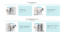
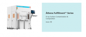
Shenzhen Angstrom Excellence Technology Co. Ltd was established in October 2020, is an expert of Semiconductor front end metrology equipment in R&D, manufacture and sales. We provide optical thin film metrology, optical critical dimension metrology, X-ray thin film metrology, X-ray critical dimension metrology, X-Ray composition and surface contamination measurement equipments, etc.
We have a professional R&D team, 80% of which holding the Doctoral or Master’s degrees. While focusing on research and development of the core technologies independently, we also devote to look for opportunities of global technical cooperation and marketing development. The R&D team have already made several technical breakthroughs and innovations in various metrology areas, the products specification are comparable with international cutting-edge products, We have 1000m2 clean room in Shenzhen, including class 1000 equipment assembly area, class 100 & 10 laboratory.
Nice to see a Shenzhen company in semiconductor equipment. So no everything is in Shanghai
Shenzhen Angstrom Excellence Technology Co. Ltd was established in October 2020, is an expert of Semiconductor front end metrology equipment in R&D, manufacture and sales. We provide optical thin film metrology, optical critical dimension metrology, X-ray thin film metrology, X-ray critical dimension metrology, X-Ray composition and surface contamination measurement equipments, etc.
We have a professional R&D team, 80% of which holding the Doctoral or Master’s degrees. While focusing on research and development of the core technologies independently, we also devote to look for opportunities of global technical cooperation and marketing development. The R&D team have already made several technical breakthroughs and innovations in various metrology areas, the products specification are comparable with international cutting-edge products, We have 1000m2 clean room in Shenzhen, including class 1000 equipment assembly area, class 100 & 10 laboratory.


Nice to see a Shenzhen company in semiconductor equipment. So no everything is in Shanghai
- Status
- Not open for further replies.
