You are using an out of date browser. It may not display this or other websites correctly.
You should upgrade or use an alternative browser.
You should upgrade or use an alternative browser.
Chinese semiconductor industry
- Thread starter Hendrik_2000
- Start date
- Status
- Not open for further replies.
Huawei's chip stack packaging patent is open!
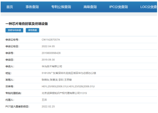
Recently, the information disclosed on the official website of the State Intellectual Property Office shows that Technologies Co., Ltd. has disclosed a patent for "a chip stacking package and terminal equipment".
According to the abstract, the present disclosure relates to the field of technology, which can solve the problem of high cost caused by the adoption of through-silicon via technology while ensuring power supply requirements.
(Screenshot from the State Patent Office)
(Screenshot from the State Patent Office)
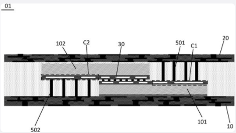
Patent documents show that the chip stack package includes:
a first chip (101) and a second chip (102) disposed between the first wiring structure (10) and the second wiring structure (20);
The active surface (S1) of the first chip (101) faces the active surface (S2) of the second chip (102);
The active surface ( S1 ) of the first chip ( 101 ) includes a first overlapping area ( A1 ) and a first non-overlapping area ( C1 ), and the active surface ( S2 ) of the second chip ( 102 ) includes a second overlapping area ( C1 ) an overlapping area (A2) and a second non-overlapping area (C2);
The first overlapping area (A1) overlaps the second overlapping area (A2), and the first overlapping area (A1) and the second overlapping area (A2) are connected;
The first non-overlapping region (C1) is connected to the second wiring structure (20);
The second non-overlapping region (C2) is connected with the first wiring structure (10).
At Huawei's 2021 performance conference held not long ago, Guo Ping, Huawei's rotating chairman, stated that in the future, Huawei may adopt a multi-core structure chip design scheme to improve performance. At the same time, using area for performance and stacking for performance, so that less advanced processes can continue to make Huawei competitive in future products.
In December last year, Huawei also invested 600 million yuan to establish a wholly-owned subsidiary of electronic manufacturing, Huawei Precision Manufacturing Co., Ltd., whose business scope is optical communication equipment manufacturing, optoelectronic device manufacturing, manufacturing and semiconductor discrete device manufacturing. . At that time, insiders said that the company had a certain scale of mass production and small batch trial production (capacity), but it was mainly used to meet the system integration needs of its own products. "It does not produce chips, it is mainly the precision manufacturing of some core devices, modules and components." At the same time, the "semiconductor discrete devices" mentioned in the business scope are mainly the packaging and testing of discrete devices. From this point of view, Huawei has a clear plan for the chip stacking route, and it may have already been put into the manufacturing process.
In addition, judging from Huawei 's major business structure adjustment in listing as a first-tier department, this indicates a reconfiguration of its strategic focus. For a long time in the past, HiSilicon was only a department under Huawei's 2012 laboratory, and the highest-end products were also used for personal use. Now, Huawei has listed HiSilicon as a first-level business unit, which largely indicates that Huawei's chip products will be adjusted from "partial commercial" to "full commercial" in the future, and Huawei will continue to increase its presence in the chip field. Talent investment and technology investment.
Recently, the information disclosed on the official website of the State Intellectual Property Office shows that Technologies Co., Ltd. has disclosed a patent for "a chip stacking package and terminal equipment".
According to the abstract, the present disclosure relates to the field of technology, which can solve the problem of high cost caused by the adoption of through-silicon via technology while ensuring power supply requirements.

(Screenshot from the State Patent Office)

(Screenshot from the State Patent Office)
Patent documents show that the chip stack package includes:
a first chip (101) and a second chip (102) disposed between the first wiring structure (10) and the second wiring structure (20);
The active surface (S1) of the first chip (101) faces the active surface (S2) of the second chip (102);
The active surface ( S1 ) of the first chip ( 101 ) includes a first overlapping area ( A1 ) and a first non-overlapping area ( C1 ), and the active surface ( S2 ) of the second chip ( 102 ) includes a second overlapping area ( C1 ) an overlapping area (A2) and a second non-overlapping area (C2);
The first overlapping area (A1) overlaps the second overlapping area (A2), and the first overlapping area (A1) and the second overlapping area (A2) are connected;
The first non-overlapping region (C1) is connected to the second wiring structure (20);
The second non-overlapping region (C2) is connected with the first wiring structure (10).
At Huawei's 2021 performance conference held not long ago, Guo Ping, Huawei's rotating chairman, stated that in the future, Huawei may adopt a multi-core structure chip design scheme to improve performance. At the same time, using area for performance and stacking for performance, so that less advanced processes can continue to make Huawei competitive in future products.
In December last year, Huawei also invested 600 million yuan to establish a wholly-owned subsidiary of electronic manufacturing, Huawei Precision Manufacturing Co., Ltd., whose business scope is optical communication equipment manufacturing, optoelectronic device manufacturing, manufacturing and semiconductor discrete device manufacturing. . At that time, insiders said that the company had a certain scale of mass production and small batch trial production (capacity), but it was mainly used to meet the system integration needs of its own products. "It does not produce chips, it is mainly the precision manufacturing of some core devices, modules and components." At the same time, the "semiconductor discrete devices" mentioned in the business scope are mainly the packaging and testing of discrete devices. From this point of view, Huawei has a clear plan for the chip stacking route, and it may have already been put into the manufacturing process.
In addition, judging from Huawei 's major business structure adjustment in listing as a first-tier department, this indicates a reconfiguration of its strategic focus. For a long time in the past, HiSilicon was only a department under Huawei's 2012 laboratory, and the highest-end products were also used for personal use. Now, Huawei has listed HiSilicon as a first-level business unit, which largely indicates that Huawei's chip products will be adjusted from "partial commercial" to "full commercial" in the future, and Huawei will continue to increase its presence in the chip field. Talent investment and technology investment.
Dinglong Lands Order From Chinese Chipmaker After Developing Own Wafer Polishing Fluid
Chinese ink products maker Dinglong said it has received an order from a mainstream domestic semiconductor maker for its self-developed wafer polishing liquid, adding that China has largely had to import these chemicals.
The unnamed buyer placed an order for 20 tons of the polishing fluid with a Dinglong subsidiary, Dingze New Material Technology, the Wuhan-based company said in a statement today. It did not disclose any financial details about the deal.
The order shows that Dingze can independently produce all the materials needed in wafer polishing, its parent company said. Until now Chinese chipmakers have had to rely on imports of the liquid, which is used to smooth out the surface of wafers, Dinglong said.
Dinglong Lands Order From Chinese Chipmaker After Developing Own Wafer Polishing Fluid

Chinese ink products maker Dinglong said it has received an order from a mainstream domestic semiconductor maker for its self-developed wafer polishing liquid, adding that China has largely had to import these chemicals.
The unnamed buyer placed an order for 20 tons of the polishing fluid with a Dinglong subsidiary, Dingze New Material Technology, the Wuhan-based company said in a statement today. It did not disclose any financial details about the deal.
The order shows that Dingze can independently produce all the materials needed in wafer polishing, its parent company said. Until now Chinese chipmakers have had to rely on imports of the liquid, which is used to smooth out the surface of wafers, Dinglong said.
Death by a thousand cuts.
A moderate victory. IP won't get choked at least. ARM architecture (embedded version) is used even in analog and microcontrollers, not just phones. Very important step forward. But it is not leading edge fab capability.
A moderate victory. IP won't get choked at least. ARM architecture (embedded version) is used even in analog and microcontrollers, not just phones. Very important step forward. But it is not leading edge fab capability.
ARM is still an proprietary IP. It is better for Chinese fabless to move away from ARM ecosystem to something like RISC-V
Actually this looks to me like bad news. ARM China was designed to insulate China from possible Western sanctions on ARM chip design licensing. By breaking ARM China from ARM they will likely cut ARM China from future core and architecture licenses.
What's the definition for illegally poaching? They stole trade secrets or something?
Afaik Taiwan made it illegal for Chinese companies to poach Taiwanese IC engineersWhat's the definition for illegally poaching? They stole trade secrets or something?
- Status
- Not open for further replies.
